SOI (silicon on insulator) LIGBT (lateral insulated gate bipolar transistor) device unit with p buried layer and longitudinal channel

A channel and device technology, applied in the direction of semiconductor devices, electrical components, circuits, etc., can solve the problems of limiting the lateral withstand voltage of the device, deteriorating the thermal characteristics of the device, aggravating the self-heating effect, etc., so as to improve the vertical withstand voltage and improve the modulation effect. , the effect of eliminating adverse effects

Active Publication Date: 2011-08-17
SERVICE CENT OF COMMLIZATION OF RES FINDINGS HAIAN COUNTY
View PDF3 Cites 14 Cited by
  • Summary
  • Abstract
  • Description
  • Claims
  • Application Information

AI Technical Summary

Problems solved by technology

The vertical withstand voltage of this device structure is not high, and it is easy to give priority to longitudinal breakdown, which seriously limits the improvement of the device's lateral withstand voltage; when a thick buried oxide layer is used to increase the vertical withstand voltage, the self-heating effect will be seriously aggravated, resulting in obvious thermal characteristics of the device. deterioration

Method used


Image

  • SOI (silicon on insulator) LIGBT (lateral insulated gate bipolar transistor) device unit with p buried layer and longitudinal channel
  • SOI (silicon on insulator) LIGBT (lateral insulated gate bipolar transistor) device unit with p buried layer and longitudinal channel
  • SOI (silicon on insulator) LIGBT (lateral insulated gate bipolar transistor) device unit with p buried layer and longitudinal channel

Examples


Embodiment Construction

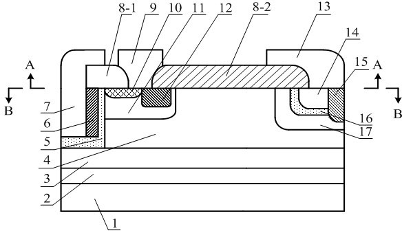
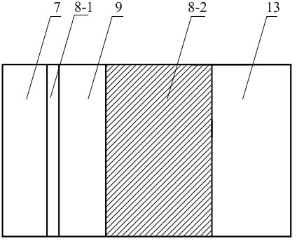
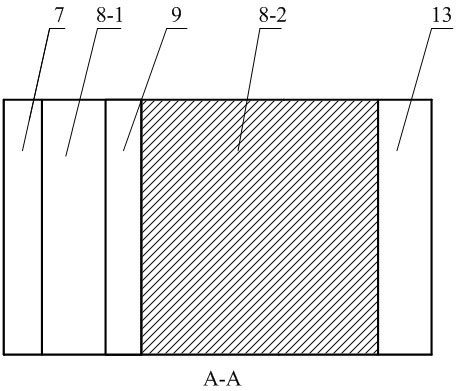
[0013] Such as figure 1 , 2 , 3 and 4, a vertical channel SOI LIGBT device unit with a p-buried layer, including a p-type semiconductor substrate 1, a buried oxide layer 2, a p-buried layer region 3, and an n-type lightly doped drift region 4 , a gate oxide layer 5, a buried oxide layer 2 covering the p-type semiconductor substrate 1, a p-buried layer region 3 covering the buried oxide layer 2, an n-type lightly doped drift region 4 and a gate oxide layer 5 arranged side by side On the p buried layer region 3, the n-type lightly doped drift region 4 is in contact with the gate oxide layer 5, and the n-type heavily doped polysilicon gate 6 is arranged next to the gate oxide layer 5, and one side of the n-type heavily doped polysilicon gate 6 It is in contact with one side of the gate oxide layer 5 .

[0014] A first p-type well region 11 and an n-type buffer region 17 are respectively embedded on both sides of the top of the n-type lightly doped drift region 4, wherein the fi...


PUM


Abstract

The invention relates to an SOI (silicon on insulator) LIGBT (lateral insulated gate bipolar transistor) device unit with a p buried layer and a longitudinal channel. The existing products restrict the improvement of the device structures and the electrical properties. The device unit comprises a p-type semiconductor substrate, a buried oxide layer and a p buried layer region in sequence, wherein a metal gate, an n-type heavily doped polysilicon gate, a gate oxide layer and an n-type lightly doped drift region are arranged at the top of the p buried layer region side by side in sequence; a first p-type well region and an n-type buffer region are respectively embedded at the two sides at the top of the n-type lightly doped drift region; an n-type cathode region and a first p well ohmic contact region are embedded at the top of the first p-type well region; a second p-type well region and an anode short-circuit point region are embedded at the top of the n-type buffer region; a second p well ohmic contact region is embedded at the top of the second p-type well region; and a first field oxide layer, a second field oxide layer, an anode metal electrode and a cathode metal electrode are arranged at the top of the device unit. The device unit has the beneficial effects of reducing the spreading resistance, improving the conductivity modulation effect of the drift region, reducing the on-state power consumption and obviously improving the thermal property of the device.

Description

technical field [0001] The invention belongs to the technical field of semiconductors, and relates to a vertical channel SOI (silicon on insulating layer) LIGBT (lateral insulated gate bipolar transistor) device unit with a P buried layer. Background technique [0002] Due to its small size, weight, high operating temperature and strong radiation resistance, low cost and high reliability, SOI LIGBT devices are used as non-contact power electronic switches or power drivers in smart power It is widely used in electronics, high temperature environment power electronics, space power electronics and vehicle power electronics. Conventional SOI LIGBTs are n - A field oxide layer is formed on the drift region; the double ion implantation polysilicon self-aligned doping technology is used to form a lateral short-channel nMOSFET and a polysilicon gate field plate near the cathode region, and an additional p + Ion implantation doping realizes the p-well well contact; the gate metal l...

Claims


Application Information

Patent Timeline
Patent Type & Authority Applications(China)
IPC IPC(8): H01L29/739H01L29/06
Inventor 张海鹏齐瑞生汪洋赵伟立刘怡新吴倩倩孔令军
Owner SERVICE CENT OF COMMLIZATION OF RES FINDINGS HAIAN COUNTY
Why Eureka
Try Eureka