Curve screen based on nanometer touch-control membrane technique and manufacturing method thereof

A nano-touch film, curved screen technology, applied in the input/output process of data processing, instruments, electrical digital data processing, etc. problem, to achieve the effect of light weight, good ductility and flexibility, and improved surface conductivity

Active Publication Date: 2011-08-31
UC NANO TECH CO LTD
View PDF7 Cites 30 Cited by
  • Summary
  • Abstract
  • Description
  • Claims
  • Application Information

AI Technical Summary

Problems solved by technology

[0002] At present, in the field of touch technology, there are touch technologies such as infrared, surface acoustic wave, surface capacitance, resistance, and optics. However, in the field of curved surface touch, these technologies have not caused revolutionary changes in the user interface. The main reason is that these Due to the complex manufacturing process and high cost of materials, touch technology cannot achieve mass production and popularization in the market
Moreover, the sensitivity of traditional touch technology becomes lower with the increase of size

Method used


Image

  • Curve screen based on nanometer touch-control membrane technique and manufacturing method thereof
  • Curve screen based on nanometer touch-control membrane technique and manufacturing method thereof
  • Curve screen based on nanometer touch-control membrane technique and manufacturing method thereof

Examples


Embodiment 1

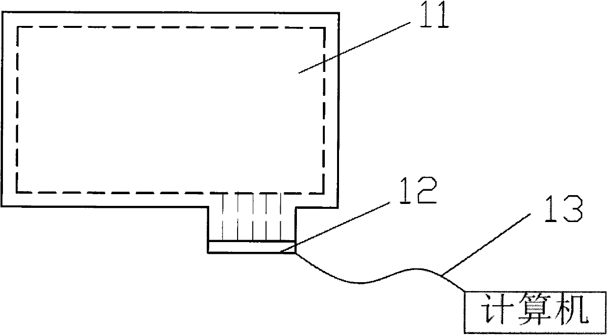
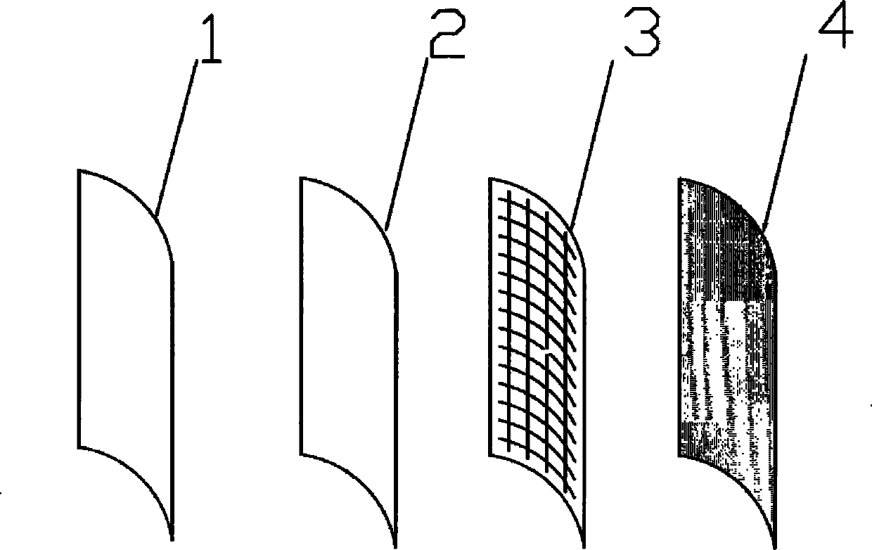
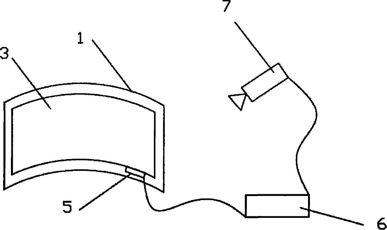
[0043] A curved screen based on nano touch film technology in this embodiment, such as figure 2 and image 3 As shown, it includes a curved substrate 1. The curved substrate 1 is a non-metallic transparent medium, which can be glass, acrylic plate or film, etc. The curvature of the curved substrate 1 is 0-180 degrees, and the bonding surface of the curved substrate 1 is The convex curved surface is sequentially attached with an adhesive film 2, a nano-touch film 3 and an imaging flexible film 4. The imaging flexible film 4 can be a holographic film or a gray film. The sensing signal of the nano-touch film 3 is collected and controlled by an integrated circuit 5 through a USB interface. Or the RS-232 interface is connected to the calculation control unit 6, and the calculation control unit 6 is connected to the projection imaging unit 7 through wired communication.

[0044] The preparation method of the curved screen of this embodiment includes the following steps:

[0045] ...

Embodiment 2

[0061] A curved screen based on nano touch film technology in this embodiment, such as Figure 4 and Figure 5 As shown, the flexible imaging device 8 is used as a curved substrate, including LCD display screens, LED display screens, OLED display screens, CNT carbon nanotube display screens, display paper or graphene display units, etc., and the curvature of the flexible imaging device 8 is 0 ~180 degrees, the adhesive surface of the flexible imaging device 8 is a concave surface, and the nano-touch film 3 is attached, and the sensing signal acquisition control integrated circuit 5 of the nano-touch film 3 passes through the cellular interface, WiFi or BlueTooth interface and the computing control unit 6 Connection, the computing control unit 6 is connected with the flexible imaging device 8 through wireless communication.

[0062] The preparation method of the curved screen of this embodiment includes the following steps:

[0063] Step 1: In an environment shielded from ele...

Embodiment 3

[0074] A curved screen based on nano-touch film technology in this embodiment is similar in structure and preparation method to Embodiments 1 and 2, except that the curved substrate or flexible imaging device is a wave-like multi-dimensional curved surface.


PUM


Abstract

The invention discloses a curve screen based on nanometer touch-control membrane technique and a manufacturing method thereof. The curve screen comprises a curve substrate, wherein the curve substrate is an arc-shaped imaging device; the radian of the curve substrate is 0-180 degrees; the curve substrate is adhered to a nanometer touch-control membrane having flexibility; a sensing signal acquisition control integrated circuit is arranged on the nanometer touch-control membrane and is connected to a computer control unit through an interface; and the computer control unit is connected to the curve substrate in a wired or wireless communication manner. In the invention, the touch control technique is realized on the curved surface. The curve screen provided by the invention is suitable fordisplay devices in different sizes. The unit cost is low, the system integration is simple, and the operation is easy, thereby ensuring that the curve screen provided by the invention is a low energy-consumption and low-carbon product.

Description

technical field [0001] The invention relates to an electronic device with touch technology, in particular to an electronic device with touch technology applied to a curved surface with a certain radian and a preparation method thereof. Background technique [0002] At present, in the field of touch technology, there are touch technologies such as infrared, surface acoustic wave, surface capacitance, resistance, and optics. However, in the field of curved surface touch, these technologies have not caused revolutionary changes in the user interface. The main reason is that these Due to the complex manufacturing process and high cost of materials, the touch technology cannot be mass-produced and popularized in the market. Moreover, the sensitivity of traditional touch technology becomes lower as the size becomes larger. The nano-imaging touch film involved in the patent application 200910181699.5, such as figure 1 As shown, it consists of two layers of PET film and a grid mat...

Claims


Application Information

Patent Timeline
Patent Type & Authority Applications(China)
IPC IPC(8): G06F3/041
Inventor 刘泽江刘轶
Owner UC NANO TECH CO LTD
Why Eureka
Try Eureka