Method for improving photoelectric detector performance by cutting band gap wavelength in lattice matching system

A photodetector and lattice matching technology, which is applied to semiconductor devices, circuits, electrical components, etc., can solve the problems of increasing optical loss and system complexity, not giving full play to device performance, and being unable to use Si detectors, etc., to achieve Reduce the intrinsic carrier concentration, good application prospects, and improve the effect of anti-interference characteristics

Inactive Publication Date: 2011-09-07
SHANGHAI INST OF MICROSYSTEM & INFORMATION TECH CHINESE ACAD OF SCI
View PDF1 Cites 11 Cited by
  • Summary
  • Abstract
  • Description
  • Claims
  • Application Information

AI Technical Summary

Problems solved by technology

When it is necessary to detect light with a wavelength greater than the bandgap wavelength of Si, such as 1.3 μm light, the Si detector is powerless.
However, it is noted that in many applications, people do not need a very wide spectral response. For example, for the detection of water vapor bands near 1.36 μm and 1.12 μm in space remote sensing, a response spectral width of about 0.1 μm is sufficient to meet the requirements; another example : Fluorescence detection of singlet oxygen in medical phototherapy research requires the central wavelength of the detected light to be 1.27 μm, and the required spectral bandwidth is only tens of nanometers. Obviously, Si detectors cannot be used in these applications
In these application systems, the detection spectrum range is often required to be as narrow as possible to reduce interference. In the case of using a wide-response spectrum detector, this needs to be realized by using narrow-band band-pass filters and other methods, which increases the optical loss. and system complexity, on the other hand, the performance of the device is not fully utilized

Method used


Image

  • Method for improving photoelectric detector performance by cutting band gap wavelength in lattice matching system
  • Method for improving photoelectric detector performance by cutting band gap wavelength in lattice matching system

Examples


Embodiment 1

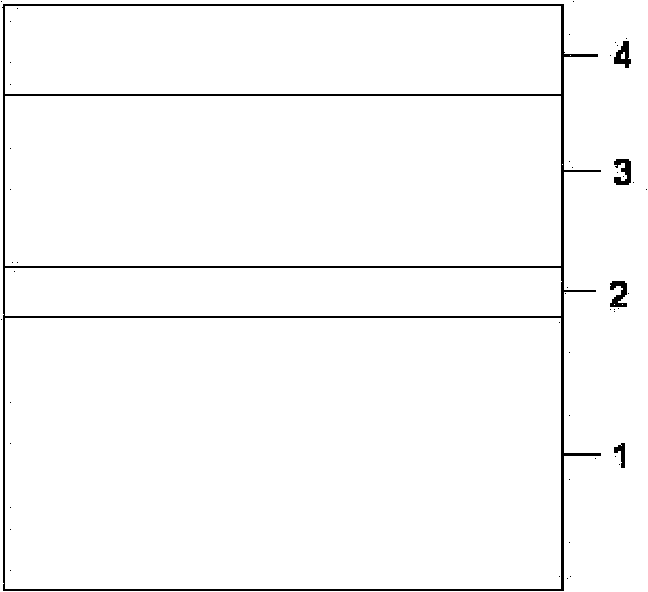
[0022] (1) A lattice-matched photodetector epitaxial structure including a buffer layer, a light absorbing layer and a wide bandgap cap layer was grown on an InP substrate by molecular beam epitaxy (MBE). The InP substrate adopts semi-insulating conductivity type; the buffer layer adopts In with narrow band gap. 0.53 Ga 0.47 As, the thickness is 200 nanometers, the doping and its concentration are determined according to the final requirements of the device; the light absorbing layer is unintentionally doped, and the thickness of the quaternary InAlGaAs set for its bandgap tailoring is 1 micron; The capping layer can be unintentionally doped, and the material is In 0.52 al 0.48 As, with a thickness of 0.5 μm;

[0023] (2) The composition of the quaternary InAlGaAs light-absorbing layer and the tailoring of the band gap are determined according to the long-wave cut-off wavelength requirements of the desired device. In the case of lattice matching with the InP substrate, the...

Embodiment 2

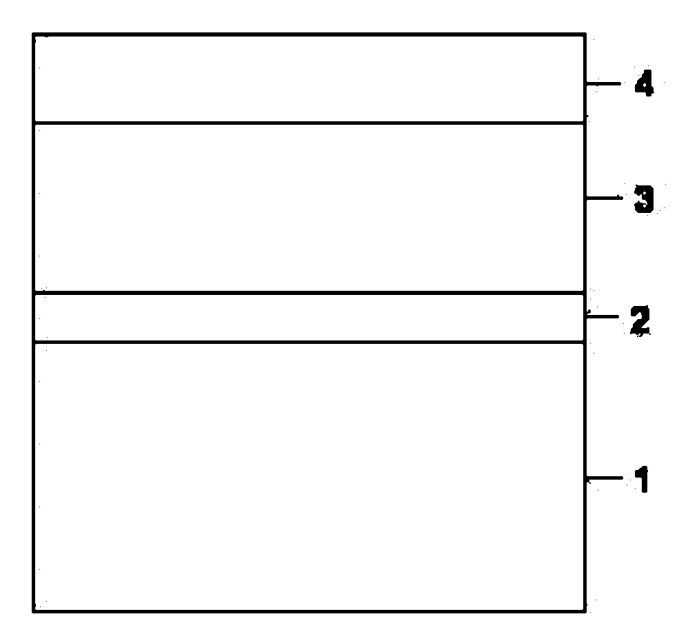
[0026] (1) A lattice-matched photodetector epitaxial structure including a buffer layer, a light absorbing layer and a wide bandgap cap layer was grown on an InP substrate by metal-organic vapor phase epitaxy (MOVPE). The InP substrate adopts N-type highly doped conductivity type; the buffer layer adopts InP material to meet the requirements of back light input, the thickness is 2000 nanometers, and the doping and its concentration can also be determined according to the final requirements of the device; the light absorbing layer is low-doped n-type, using quaternary InGaAsP set for its bandgap tailoring, with a thickness of 3 microns; the wide bandgap cap layer is a highly doped p-type material, InP, with a thickness of 1 micron;

[0027] (2) The composition of the quaternary InGaAsP light-absorbing layer and the tailoring of the band gap are determined according to the long-wave cut-off wavelength requirements of the desired device. In the case of lattice matching with the I...


PUM


Abstract

The invention relates to a method for improving photoelectric detector performance by cutting band gap wavelength in lattice matching system. The method comprises the following steps of: growing a buffer layer, a light absorption layer and a wide band gap cap layer which hare matched with lattices on a substrate by using an MBE (molecular beam epitaxy) method or metallorganics vapour phase epitaxy method to obtain an epitaxial structure of a photoelectric detector, wherein the band gap of the light absorption layer can be cut and set during the growth process, and the wide band gap is selected on the premise of meeting cut-off wavelength requirement of the long wave end of the photoelectric detector. According to the invention, the material growing method is simple; by cutting and setting the band gap of the light absorption layer of the photoelectric detector, the device performance can be obviously improved under the condition of basically not changing the original design of the device, and the detectivity can be enhanced by more than three times. The method is not only suitable for manufacturing photoelectric detectors in different kinds of III-V compound material systems, but also suitable for manufacturing other types of photoelectric devices and electronic devices; and the application of the method can be widened to other material systems. The method has a good application prospect.

Description

technical field [0001] The invention belongs to the field of epitaxial structures of semiconductor photodetectors, in particular to a method for improving the performance of photodetectors by clipping bandgap wavelengths on a lattice matching system. Background technique [0002] Semiconductor photodetectors are generally quantum detectors. Its invention has a history of more than 100 years. It can use various semiconductor materials and has important applications in many fields. The structure of semiconductor photodetectors has developed from simple bulk materials to complex microstructure materials such as heterojunctions, quantum wells, and superlattices. Visible, near-infrared, mid-infrared and even far-infrared bands, material systems also include VI, III-V, II-VI, IV-VI and organic compounds, etc., as well as photoconductive, photovoltaic and other types, and so on. The common ones are photovoltaic photodetectors based on pn junctions. At present, typical pn junction...

Claims


Application Information

Patent Timeline
Patent Type & Authority Applications(China)
IPC IPC(8): H01L31/18H01L31/0256H01L31/0304
CPCY02P70/50
Inventor 张永刚顾溢
Owner SHANGHAI INST OF MICROSYSTEM & INFORMATION TECH CHINESE ACAD OF SCI
Why Eureka
Try Eureka