Graphene field effect transistor with photoconduction effect and infrared detector

A field-effect transistor and graphene technology, applied in the graphene field, can solve the problems of high application cost, achieve low operating cost, avoid complex production process, and low power consumption

Inactive Publication Date: 2011-09-14
FUDAN UNIV
View PDF2 Cites 30 Cited by
  • Summary
  • Abstract
  • Description
  • Claims
  • Application Information

AI Technical Summary

Problems solved by technology

At present, among infrared detectors of various bands, whether it is InGaAs-based, InSb-based, or quantum well-type detection QWIP and mercury cadmium telluride (M

Method used


Image

  • Graphene field effect transistor with photoconduction effect and infrared detector
  • Graphene field effect transistor with photoconduction effect and infrared detector
  • Graphene field effect transistor with photoconduction effect and infrared detector

Examples


Embodiment Construction

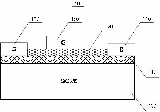
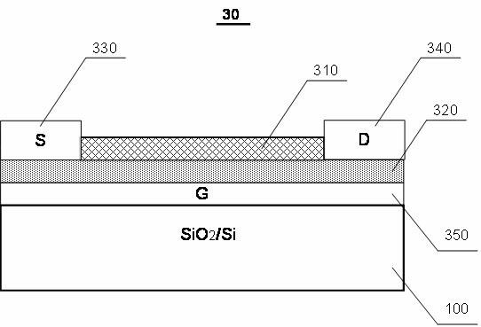
[0026] The present invention will be further described below in conjunction with the accompanying drawings and reference examples. The present invention provides preferred embodiments, but should not be construed as limited to the embodiments set forth herein. In the drawings, the thicknesses of layers and regions are exaggerated for clarity, but as schematic diagrams, they should not be considered to strictly reflect the proportional relationship of geometric dimensions.

[0027] The referenced figures are schematic illustrations of idealized embodiments of the invention, and the illustrated embodiments of the invention should not be construed as limited to the particular shapes of regions shown in the figures but are to include resulting shapes, such as manufacturing-induced deviations. For example, the curves obtained by dry etching usually have curved or rounded characteristics, but in the illustrations of the embodiments of the present invention, they are all represented ...


PUM

PropertyMeasurementUnit
Wavelengthaaaaaaaaaa
Thicknessaaaaaaaaaa

Abstract

The invention belongs to the technical field of graphene, and particularly discloses a graphene field effect transistor (GFET) with photoconduction effect and an infrared detector. The GFET comprises a graphene channel layer which generates photoconduction effect under infrared radiation operatively so as to change the electric characteristic of the GFET; the GFET is high in sensitivity and low in power consumption. The infrared detector manufactured by using the GFET does not need a refrigerating system, has low operating cost and is ultralight and ultrastable, the infrared absorbing bandwidth of the infrared detector can be adjusted according to the practical application need; and the problem that the traditional infrared detector is manufactured by complicated process and has hypertoxicity are also avoided; in addition, the infrared detector disclosed by the invention is especially suitable for application in sky-survey infrared detection.

Description

technical field [0001] The invention belongs to the technical field of graphene, in particular to a graphene field effect transistor, in particular to a graphene effect transistor with a photoconductive effect and an infrared detector based on the effect transistor. Background technique [0002] With the continuous extension and depth of Moore's law, the device size of silicon-based integrated circuits is getting closer and closer to the physical limit, and the international semiconductor technology community has proposed Beyond Silicon (Beyond Silicon) technologies, among which Graphene (Graphene) It is considered to be the most promising material to replace silicon. [0003] Graphene is a two-dimensional crystal composed of carbon atoms on a single-layer honeycomb crystal lattice, and the thickness of a single-layer graphite is about 0.35 nanometers. figure 1 A schematic diagram of the basic structure of graphene. Currently, graphite with less than ten layers is regarded...

Claims


Application Information

Patent Timeline
IPC IPC(8): H01L31/113H01L31/028
Inventor 周鹏孙清清吴东平张卫
Owner FUDAN UNIV
Why Eureka
Try Eureka