Resin composition for electronic component encapsulation and electronic component device

A technology of resin composition and electronic components, which is applied in the direction of electrical components, electrical solid devices, semiconductor/solid device parts, etc., can solve the problems of package warpage and achieve the effect of warpage reduction

Inactive Publication Date: 2011-09-21
NITTO DENKO CORP
View PDF4 Cites 10 Cited by
  • Summary
  • Abstract
  • Description
  • Claims
  • Application Information

AI Technical Summary

Problems solved by technology

For example, in the case of a semiconductor device having a single-sided packaging structure called a ball grid array (BGA), since only one side of a semiconductor element mounted on a substrate is packaged, a problem may occur due to The shrinkage difference between the encapsulation resin of the product and the substrate generates stress between the encapsulation resin and the substrate, so warpage occurs on the package due to the stress

Method used


Image

  • Resin composition for electronic component encapsulation and electronic component device
  • Resin composition for electronic component encapsulation and electronic component device
  • Resin composition for electronic component encapsulation and electronic component device

Examples


Embodiment 1~4, comparative example 1 and 2

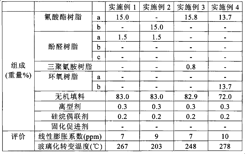
[0065] Various ingredients shown in Tables 1 and 2 below were blended in the ratios shown in the tables, and melt-kneaded at 100°C for 3 minutes using a roller kneader. Then, the molten product was cooled and then pulverized to prepare a resin composition.

[0066] [Linear expansion coefficient, glass transition temperature]

[0067] Using the obtained resin composition, a cured product (length: 20 mm, width: 3 mm, thickness: 3 mm) was prepared by transfer molding (175° C.×3 minutes). The obtained cured product was subjected to post-curing (175° C.×5 hours, then 200° C.×4 hours, and finally 250° C.×4 hours) to prepare test pieces. The linear expansion coefficient and the glass transition temperature were determined using a TMA apparatus (model MG800GM) manufactured by Rigaku Corporation at a temperature increase rate of 5° C. / min. Tables 1 and 2 show the results.

[0068] Table 1

[0069]

[0070] Table 2

[0071]

[0072] The coefficient of linear expansion of a ce...


PUM

PropertyMeasurementUnit
melting pointaaaaaaaaaa
softening pointaaaaaaaaaa

Abstract

The present invention relates to a resin composition for electronic component encapsulation and an electronic component device, the resin composition including: A: a cyanate ester resin; B: at least one selected from the group consisting of a phenol resin, a melamine compound and an epoxy resin; and C: an inorganic filler.

Description

technical field [0001] The present invention relates to a resin composition for electronic component encapsulation, which suppresses warpage of a resin-encapsulated electronic component device and also has excellent heat resistance. Background technique [0002] Recently, with regard to electronic component devices obtained by resin-encapsulating electronic components such as semiconductor elements, capacitors, transistors, and sensor devices, thinning and upsizing have been demanded. For example, in the case of a semiconductor device having a single-sided packaging structure called a ball grid array (BGA), since only one side of a semiconductor element mounted on a substrate is packaged, a problem may occur due to The shrinkage difference between the encapsulating resin of the product and the substrate generates stress between the encapsulating resin and the substrate, so warpage occurs in the package due to the stress. In order to suppress the warpage, it is studied that ...

Claims


Application Information

Patent Timeline
Patent Type & Authority Applications(China)
IPC IPC(8): C08L79/04C08L61/06C08L63/00C08K5/3492C08K7/18C08K3/36H01L23/29
CPCC08L61/04C08G73/0644C08L79/04H01L23/296C08G73/0655H01L23/295C08L63/00C08K3/0033H01L23/293H01L2924/0002C08K3/013C08L2666/22C08L2666/20H01L2924/00C08L67/06C08L61/28C08K3/00H01L23/29
Inventor 北川祐矢田渊康子
Owner NITTO DENKO CORP
Why Eureka
Try Eureka