Optical waveguide for optical connector, optical connector using same, and method of manufacturing optical waveguide for optical connector

An optical connector and waveguide technology, applied in the coupling, optical, optical and other directions of optical waveguides, can solve the problems of increasing optical coupling loss, large deviation of the width direction of the optical waveguide, inconsistent optical axes, etc., to prevent optical coupling loss. The effect of increasing the number of products, small variation between products, and high reproducibility

Active Publication Date: 2011-09-21
NITTO DENKO CORP
View PDF3 Cites 5 Cited by
  • Summary
  • Abstract
  • Description
  • Claims
  • Application Information

AI Technical Summary

Problems solved by technology

[0009] However, due to the performance limit of the dicing process performed by a dicing machine, the optical waveguide for an optical connector obtained by individually separating the dicing machine as described above suffers from low dimensional accuracy, and especially large variations in the width direction of the optical waveguide. The problem
In this way, if the variation in the dimension of the width direction of the optical waveguide is large, even if the optical waveguide is inserted and fixed in the through-hole for fixing the optical waveguide formed at a predetermined position of the ferrule, and the guide pin or the like is used to adjust the While the cores connect the optical connectors facing each other, the optical axes of the cores in the abutting optical waveguide do not coincide, which increases the optical coupling loss
[0010] In addition, compared with the above-mentioned case of using a dicing machine, the optical waveguide for optical connectors separated by laser has improved dimensional accuracy in the width direction, but the performance of the optical waveguide decreases due to the heating of the laser.
In addition, unlike a dicing machine, a laser has the advantage of being able to separate optical waveguides in a curved line, but has the disadvantage of requiring an additional cleaning process to remove processing residue remaining after processing

Method used


Image

  • Optical waveguide for optical connector, optical connector using same, and method of manufacturing optical waveguide for optical connector
  • Optical waveguide for optical connector, optical connector using same, and method of manufacturing optical waveguide for optical connector
  • Optical waveguide for optical connector, optical connector using same, and method of manufacturing optical waveguide for optical connector

Examples


Embodiment 1

[0094] 〔Fabrication of Under Cladding〕

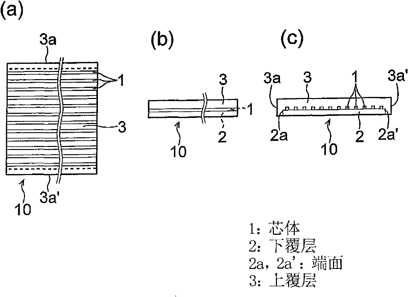
[0095] First of all, using a spin coater The spin coating method applied the material for forming the under-cladding layer used in Example 1 above to the glass substrate 2 365nm radiation To make an exposure. The quartz photomask M1 has openings of a square pattern (width 2.88 mm×length 102.0 mm) corresponding to the under cladding layer, and is separated from each other on a line parallel to the length (long side) direction of the square opening Two openings are formed in a pattern corresponding to the ring-shaped alignment mark A (diameter 1 mm, width 50 μm). Immediately afterwards, heat treatment was performed at 150°C for 10 minutes. Then, after using Y-butyrolactone After performing immersion development for 3 minutes to dissolve and remove the unexposed part, heat treatment is performed at 150° C. for 10 minutes to form an under cladding layer and two ring-shaped alignment marks A on the substrate. The cross-sectional size of th...

Embodiment 2

[0105] 〔Fabrication of Under Cladding〕

[0106] First of all, using a spin coater The spin coating method applied the material for forming the under-cladding layer used in Example 1 above to the glass substrate 2 365nm radiation For exposure, the quartz photomask M1 has an opening with a square pattern (width 2.90 mm × length 102.0 mm) corresponding to the under cladding layer, and is on a line parallel to the length (long side) direction of the square opening Openings in a pattern corresponding to the ring-shaped alignment mark A (diameter 1 mm, width 50 μm) are formed at two places separated from each other. Immediately afterwards, heat treatment was performed at 100°C for 15 minutes. Then, after using Y-butyrolactone After performing immersion development for 3 minutes to dissolve and remove the unexposed parts, heat treatment at 150° C. for 15 minutes was performed to form the under cladding layer and two ring-shaped alignment marks A on the substrate. The cross-sectional...

Embodiment 3

[0116] 〔Fabrication of Under Cladding〕

[0117] First of all, using a spin coater The spin coating method applied the material for forming the under-cladding layer used in Example 3 above to the glass substrate 2 365nm radiation For exposure, the quartz photomask M1 has an opening with a square pattern (width 2.885 mm×length 102.0 mm) corresponding to the under cladding layer, and is positioned on a line parallel to the length (long side) direction of the square opening Openings in a pattern corresponding to the ring-shaped alignment mark A (diameter 1 mm, width 50 μm) are formed at two places separated from each other. Next, heat treatment is performed at 70°C×15 minutes. Then, after using Y-butyrolactone After performing immersion development for 3 minutes to dissolve and remove the unexposed parts, heat treatment at 150° C. for 15 minutes was performed to form the under cladding layer and two ring-shaped alignment marks A on the substrate. The cross-sectional dimensions of ...


PUM


Abstract

Disclosed is inexpensive optical waveguide for an optical connector which is accurately positioned across the width of cores when inserted in and fixed in an optical waveguide fixing through hole of a ferrule to provide low optical coupling loss when connected, an optical connector using the same, and a method of manufacturing the same. An optical waveguide for an optical connector includes cores, an under cladding layer, and an over cladding layer. The strip-shaped optical waveguide has a longitudinal end portion configured to be fixed in a predetermined through hole provided in a ferrule of an optical connector. The cores are formed on the under cladding layer by a photolithographic method. The over cladding layer is formed with respect to the positions of the cores or positioning alignment marks by a photolithographic method. The over cladding layer covers the cores, and the under cladding layer including crosswise end surfaces thereof and the width of the over cladding layer is approximately equal to that of the hole for fixing the optical waveguide.

Description

Technical field [0001] The present invention relates to an optical waveguide for an optical connector, an optical connector using the optical waveguide, and a method for manufacturing the optical waveguide for the optical connector. Background technique [0002] In recent years, due to the integration and large-scale increase of electronic equipment, heat generation and power consumption of electrical wiring, which are often used to connect between boards in the equipment and between chips on the board, have become a problem. Therefore, an optical wiring (optical interconnection) technology for replacing the above-mentioned electrical wiring with a lightweight, low-heat-generating, and flexible polymer optical waveguide is being developed. [0003] In this optical wiring, the optical connector used to connect the boards and the like consists of a strip-shaped optical waveguide and a ferrule (ferrule) mounted on the longitudinal end of the optical waveguide. The connection of a pre...

Claims


Application Information

Patent Timeline
Patent Type & Authority Applications(China)
IPC IPC(8): G02B6/122G02B6/38G02B6/138
CPCG02B6/138G02B6/1221G02B6/3897G02B6/3885
Inventor 宗和范藤泽润一辻田雄一
Owner NITTO DENKO CORP
Why Eureka
Try Eureka