Method for enlarging metal interconnected lithography process window

A photolithography process and metal interconnection technology, which is applied in the direction of electrical components, semiconductor/solid-state device manufacturing, circuits, etc., can solve the problems of metal interconnection failure, limited photolithography process window, collapse, etc., and achieve the goal of reducing the square resistance value Differences, expanding the photolithography process window, and improving the effect of consistency

Inactive Publication Date: 2011-09-21
SEMICONDUCTOR MANUFACTURING INTERNATIONAL (BEIJING) CORP +1
View PDF3 Cites 4 Cited by
  • Summary
  • Abstract
  • Description
  • Claims
  • Application Information

AI Technical Summary

Problems solved by technology

However, if the adhesion (adhesion) between the low-temperature oxide layer and the organic bottom anti-reflective coating is not high enough, after exposure with a smaller line width, it may cause excessive corrosion of the organic bottom anti-reflective coating, which will As a result, the pattern under the organic bottom anti-reflective coating cannot maintain the photoresist pattern and collapse during the etching step, resulting in the failure of the subsequent metal interconnection, which limits the photolithography process window of the metal interconnection in the existing process

Method used


Image

  • Method for enlarging metal interconnected lithography process window
  • Method for enlarging metal interconnected lithography process window

Examples


Embodiment Construction

[0011] In order to make the purpose and features of the present invention more comprehensible, the specific implementation manners of the present invention will be further described below in conjunction with the accompanying drawings.

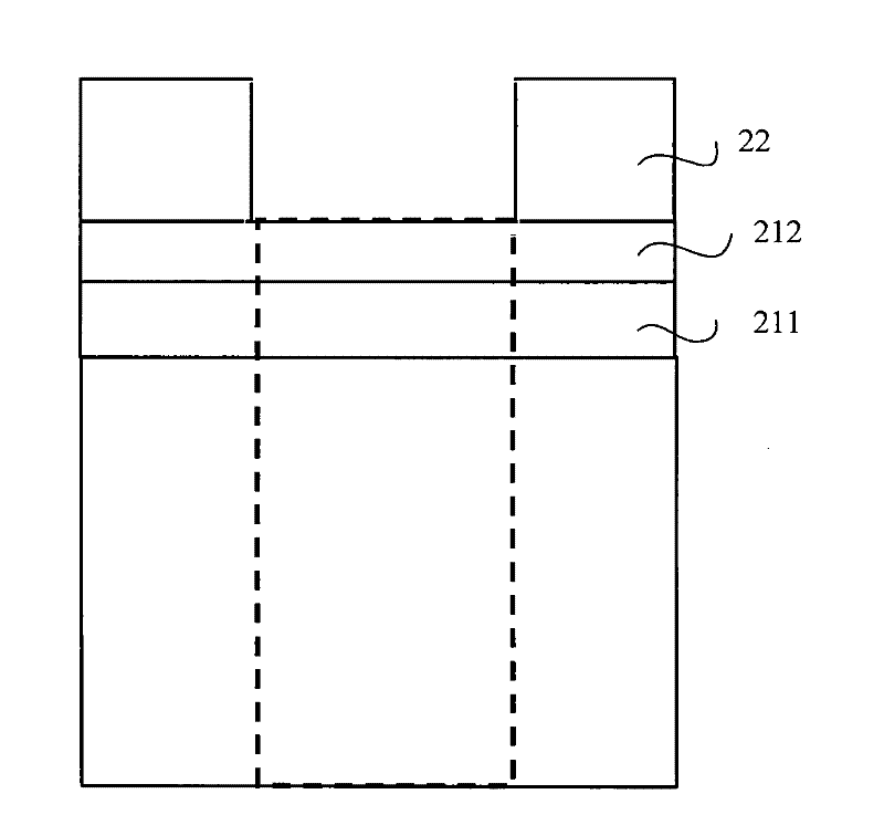
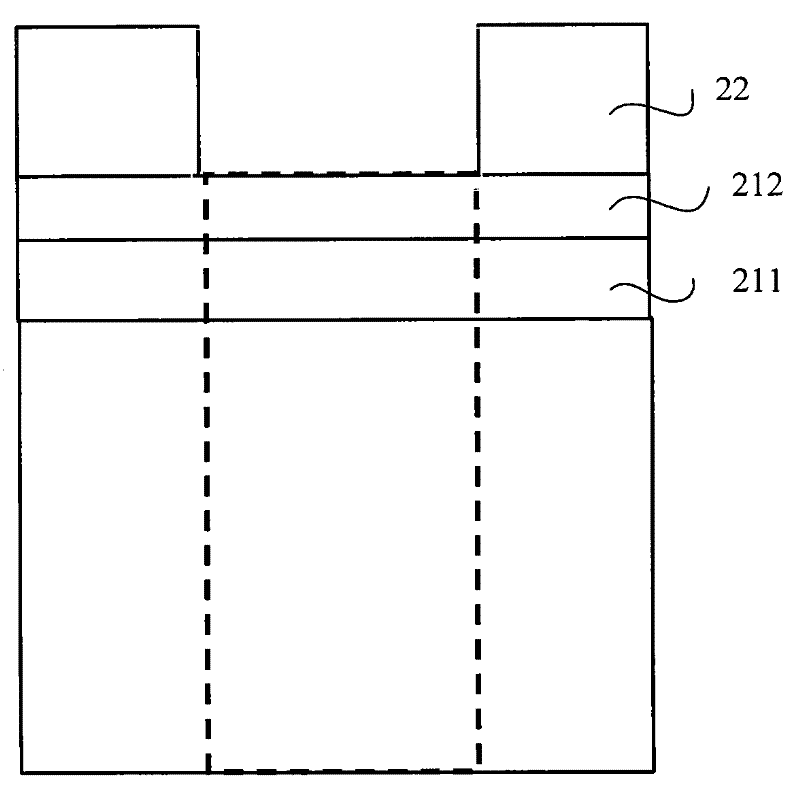
[0012] As mentioned in the background art, the adhesion between the low-temperature oxide layer and the organic bottom anti-reflective coating in the prior art is not high enough. After exposure with a smaller line width, it may cause damage to the organic bottom anti-reflective coating. Excessive corrosion will cause the photoresist pattern on the organic bottom anti-reflective coating to fail to maintain and collapse, resulting in the failure of the subsequently formed metal interconnection.

[0013] The core idea of ​​the present invention is that by treating the surface of the low-temperature oxide layer with active gas plasma, the surface of the low-temperature oxide layer becomes flatter and denser, and the adhesion between the low-tempera...


PUM


Abstract

The invention discloses a method for enlarging a metal interconnected lithography process window. The metal interconnection is realized through a dual-damascenes structure which comprises through holes and grooves. The grooves are formed from a hard mask by a lithography process. The hard mask comprises a low-temperature oxide layer and an organic bottom antireflection coating which is formed above the low-temperature oxide layer, wherein after the low-temperature oxide layer is formed by a deposition process, the surface of the low-temperature oxide layer is processed by using active gas plasmas so as to improve the adhesion between the low-temperature oxide layer and the organic bottom antireflection coating.

Description

technical field [0001] The invention relates to the technical field of silicon semiconductor devices, in particular to a method for enlarging the photolithography process window of metal interconnection. Background technique [0002] With the continuous improvement of the integration of components in integrated circuits, the size of components is continuously reduced, which also puts forward higher requirements for interconnection technology. The industry usually adopts a dual damascene structure to realize metal interconnection. According to the double damascene structure, a via hole and a trench are successively formed in the dielectric layer, an upper interconnection is formed in the trench, and the upper interconnection is connected to the lower interconnection or the substrate through the via hole. During the formation of the dual damascene structure, the gap needs to be filled after etching the via hole for trench lithography. When performing trench lithography, a th...

Claims


Application Information

Patent Timeline
Patent Type & Authority Applications(China)
IPC IPC(8): H01L21/768
Inventor 赵保军
Owner SEMICONDUCTOR MANUFACTURING INTERNATIONAL (BEIJING) CORP
Why Eureka
Try Eureka