Method for making contact hole

A contact hole and shrink layer technology, which is used in semiconductor/solid-state device manufacturing, electrical components, electrical solid-state devices, etc., to achieve good uniformity

Inactive Publication Date: 2011-09-21
SEMICON MFG INT (SHANGHAI) CORP +1
View PDF3 Cites 10 Cited by
  • Summary
  • Abstract
  • Description
  • Claims
  • Application Information

AI Technical Summary

Problems solved by technology

However, for the next-generation 32nm node process, the critical dimension of the contact hole after etching is required to be about 40nm. However, due to the limitation of the exposure limit of the photolithography machine, the critical dimension that can be achieved after the development of the photoresist layer is 80nm. Therefore, it is required to achieve a shrinkage of 40nm, which is a big challenge for the existing technology

Method used


Image

  • Method for making contact hole
  • Method for making contact hole
  • Method for making contact hole

Examples


Embodiment Construction

[0031] In the following description, numerous specific details are given in order to provide a more thorough understanding of the present invention. It will be apparent, however, to one skilled in the art that the present invention may be practiced without one or more of these details. In other examples, some technical features known in the art are not described in order to avoid confusion with the present invention.

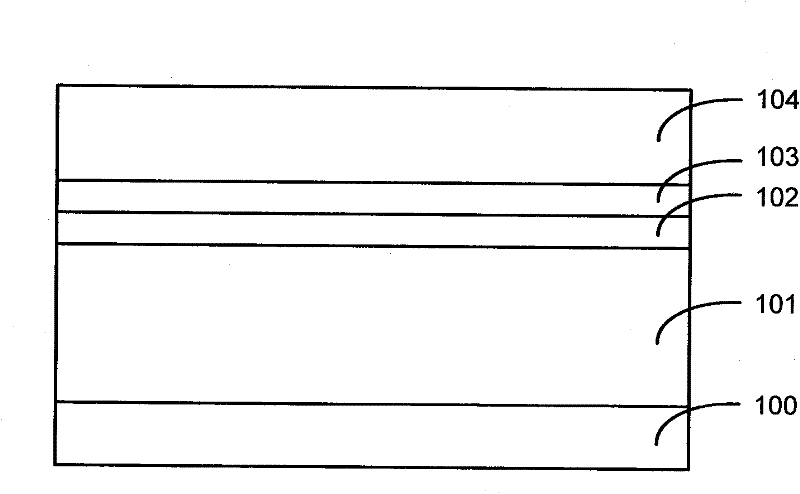
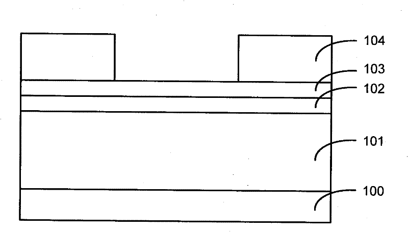
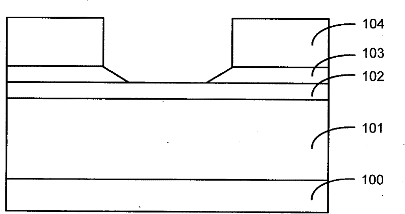
[0032] In order to thoroughly understand the present invention, detailed steps will be proposed in the following descriptions, so as to illustrate how the present invention solves the need to achieve 40nm or even greater shrinkage in the dry etching process of contact holes at the 32nm technology node to produce Difficulties with contact holes of the required diameter. Obviously, the practice of the invention is not limited to specific details familiar to those skilled in the semiconductor arts. Preferred embodiments of the present invention are described in d...


PUM

PropertyMeasurementUnit
thicknessaaaaaaaaaa
thicknessaaaaaaaaaa
thicknessaaaaaaaaaa

Abstract

The invention discloses a method for making a contact hole, which comprises the steps of: forming an etching stop layer on a front-end device layer; forming a dielectric layer on the etching stop layer; forming a contraction layer on the dielectric layer; forming a bottom anti-reflection coating on the contraction layer; coating a photoetching glue layer with patterns on the bottom anti-reflection coating; etching the bottom anti-reflection coating by using the photoetching glue layer with patterns as a mask to form a first opening; etching the contraction layer by using etching gases including fluorohydrocarbon gas and oxygen by using the photoetching glue layer with patterns and the bottom anti-reflection coating as masks to form a second opening with a tapered incline side wall; etching the dielectric layer to the upper layer of the etching stop layer by using the contraction layer as a mask; and removing the bottom anti-reflection coating and the contraction layer to form the contact hole. According to the method disclosed by the invention, 40nm and even larger contraction amount can be effectively realized, and better key size uniformity can be obtained.

Description

technical field [0001] The invention relates to a semiconductor device manufacturing process, in particular to a method for making a contact hole. Background technique [0002] The manufacture of semiconductor integrated circuits is an extremely complex process, the purpose of which is to reduce the various electronic components and circuits required for a specific circuit on a small-area wafer. Among them, the various components must be electrically connected through appropriate interconnecting wires, so as to exert desired functions. [0003] As the manufacture of integrated circuits develops toward ultra-large-scale integrated circuits (ULSI), the internal circuit density is increasing. As the number of components contained in the chip continues to increase, the available space for surface wiring is actually reduced. The solution to this problem is to adopt a multi-layer metal wire design, and use a multi-layer connection in which a multi-layer insulating layer and a con...

Claims


Application Information

Patent Timeline
Patent Type & Authority Applications(China)
IPC IPC(8): H01L21/768H01L23/522
Inventor 孙武王新鹏张世谋黄怡
Owner SEMICON MFG INT (SHANGHAI) CORP
Why Eureka
Try Eureka