
Optical-fibre-embedded glass plate and manufacturing method thereof

A technology of glass plate and optical fiber, which is applied in the coupling of optical waveguide, optical waveguide and light guide, etc., can solve the problems of large optical loss, difficult mode matching, large dielectric constant and dielectric loss, etc., so as to improve frequency and speed, and facilitate Large-scale mass production, good effect of high-frequency electrical performance

Inactive Publication Date: 2011-09-28
INST OF MICROELECTRONICS CHINESE ACAD OF SCI
View PDF9 Cites 4 Cited by
  • Summary
  • Abstract
  • Description
  • Claims
  • Application Information

AI Technical Summary

Problems solved by technology

However, silicon substrates also have disadvantages: (1) Silicon is a semiconductor. In TSV interconnection, it is necessary to make multi-layer structures such as insulating layers and barrier layers on the side walls. The process is complicated, the preparation time is long and the production cost is high.
(2) The dielectric constant and dielectric loss of silicon are relatively large, which seriously affects the high-frequency transmission performance
(3) Silicon is opaque, has a large difference in refractive index with optical fibers and optical devices, and the mode is not easy to match, and the coupling efficiency is low
However, the above two structures do not have waveguides or optical fibers in the vertical direction, so there are defects such as large optical loss and easy mode changes.
On the other hand, there are certain technical difficulties in arranging waveguides or optical fibers in the vertical direction of the glass substrate.
For example, the current hole-filling process is difficult to vertically fill the waveguide into the glass substrate without affecting the performance of the waveguide, so it cannot meet the requirements of a large number of vertical interconnections between chips in the three-dimensional package.

Method used


Image

  • Optical-fibre-embedded glass plate and manufacturing method thereof
  • Optical-fibre-embedded glass plate and manufacturing method thereof
  • Optical-fibre-embedded glass plate and manufacturing method thereof

Examples


Embodiment 1

[0072] Figure 4a to Figure 4h The process flow of the manufacturing method of the glass plate structure of Example 1 is shown. in Figure 4h It is a structural schematic diagram of the glass plate of Example 1.

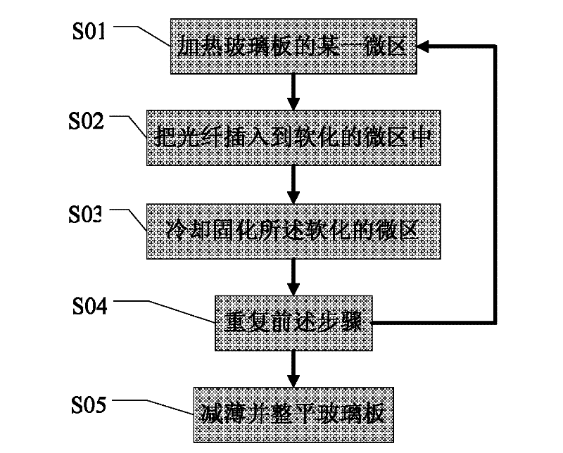
[0073] The manufacturing method of the glass plate structure of the embodiment of the present invention 1 comprises the following steps:

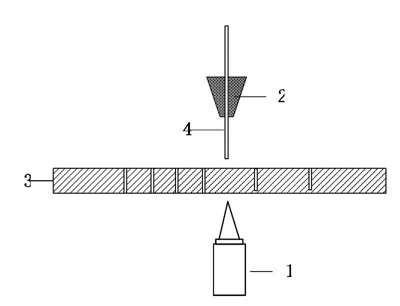
[0074] Step S101, such as Figure 4a As shown, choose Corning Pyrex 7740 glass plate 101, the size is 4 inches disc, the thickness is 400-500 microns, choose silica fiber as embedded fiber material 301, choose laser as micro-zone heating device 203, one has the function of holding and conveying A mechanical device capable of three-axis movement is used as an optical fiber insertion device 201 .

[0075] Step S102 , aligning the laser 203 and the optical fiber insertion device 201 at a certain micro-area position 202 of the glass substrate 101 through an optical system.

[0076] Step S103, such as Figure 4b As shown, the las...

Embodiment 2

[0085] Figure 5 A schematic diagram of the glass plate structure of Example 2 is shown.

[0086] The manufacturing method of the glass plate of Example 2 is mostly similar to that of Example 1, the difference is that after the glass plate is fabricated, different connection mechanisms for connecting with external devices or optical fibers are fabricated, so the same steps are briefly described.

[0087] The manufacturing method of the glass plate structure of the embodiment of the present invention 2 comprises the following steps:

[0088] Step S201, select a glass plate with metal-filled through-glass vias, such as SCHOTT HermeS TM Glass base board. The size is a 4-inch disc, and the thickness is 400-500 microns. The quartz optical fiber is selected as the embedded fiber material 301, the laser is selected as the micro-area heating device 203, and a mechanical device with holding and transporting functions that can move in three axes is used as the metal wire. Insert device...

Embodiment 3

[0093] Figure 6a to Figure 6c The process flow of the manufacturing method of the glass plate structure of Example 3 is shown. in Figure 6c It is a structural schematic diagram of the glass plate of Example 3.

[0094] The manufacturing method of the glass plate structure of the embodiment of the present invention 3 comprises the following steps:

[0095] Step S301, such as Figure 4a As shown, choose Corning Pyrex 7740 glass plate 101, the size is 4 inches disc, the thickness is 400-500 microns, choose silica fiber as embedded fiber material 301, choose laser as micro-zone heating device 203, one has the function of holding and conveying A mechanical device capable of three-axis movement is used as the wire insertion device 201 .

[0096] Step S302 , through the optical system, align the laser 203 and the fiber insertion device 201 with a micro-region 202 on the glass plate 101 where the fiber needs to be embedded and where both ends of the fiber need to be exposed.

...


PUM

PropertyMeasurementUnit
diameteraaaaaaaaaa
thicknessaaaaaaaaaa

Abstract

The invention discloses an optical-fibre-embedded glass plate and a manufacturing method thereof. The optical-fibre-embedded glass plate comprises a glass plate having an upper surface and a lower surface, wherein at least one optical fibre is vertical to a surface of the glass plate and embedded into the glass plate; and at least one end of the optical fibre is exposed out of the upper surface or the lower surface of the glass plate. The optical-fibre-embedded glass plate can realize vertical transmission of a high-speed light signal between chips. The optical-fibre-embedded glass plate is simple in manufacturing process and low in cost and solves the problems that the glass substrate is difficult to hole and has a complicated hole-filling process.

Description

technical field [0001] The invention relates to the technical field of microelectronic packaging, in particular to a glass plate embedded with optical fibers and a method for manufacturing the glass plate embedded with optical fibers, so as to realize high-speed optical interconnection structures in three-dimensional packaging or multilayer stack packaging. Background technique [0002] With the rapid development of data communication services and the Internet, the demand for bandwidth increases explosively, and people's requirements for computing speed and communication speed of electronic products are greatly increased. At the same time, people require electronic products to be more miniaturized, multi-functional, and run faster. This requires electronic systems to be smaller and smaller, with higher integration, more functions, and faster communication between chips. The technical requirements are also getting higher and higher. The traditional two-dimensional packaging ...

Claims


Application Information

Patent Timeline
Patent Type & Authority Applications(China)
IPC IPC(8): G02B6/12G02B6/42
Inventor 于大全孙瑜戴风伟
Owner INST OF MICROELECTRONICS CHINESE ACAD OF SCI
Learn More