Method for optimizing light gathering ability of micro-lens array of back-illuminated infrared detector

A technology of microlens array and light-gathering ability, which is applied in the direction of lenses, instruments, optics, etc., can solve the problems of little research on the light-gathering ability of microlenses, and achieve improved device performance, reduced optical crosstalk, and easy to use Effect

Inactive Publication Date: 2013-01-09
SHANGHAI INST OF TECHNICAL PHYSICS - CHINESE ACAD OF SCI
View PDF0 Cites 6 Cited by
  • Summary
  • Abstract
  • Description
  • Claims
  • Application Information

AI Technical Summary

Problems solved by technology

Although there have been a lot of reports on microlens arrays at home and abroad so far, they basically discuss the manufacturing process of microlenses, the types of microlenses such as refractive lenses, diffractive lenses, and hybrid lenses, and how to optimize microlenses. The light-gathering ability of

Method used


Image

  • Method for optimizing light gathering ability of micro-lens array of back-illuminated infrared detector
  • Method for optimizing light gathering ability of micro-lens array of back-illuminated infrared detector
  • Method for optimizing light gathering ability of micro-lens array of back-illuminated infrared detector

Examples


Embodiment Construction

[0020] The specific embodiment of the present invention is described in detail below in conjunction with accompanying drawing:

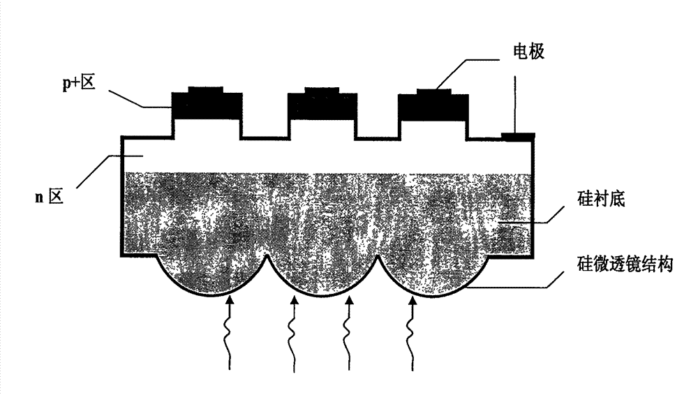
[0021] 1. First construct a two-dimensional simulated device model based on the indium antimonide infrared focal plane detector array, that is, p + -on-n type indium antimonide infrared focal plane detector array structure: the p-region thickness is 0.8 μm and the doping concentration is 10 17 cm -3 , the n-region thickness is 12.2μm and the doping concentration is 10 15 cm -3 , the substrate material is a silicon material with a thickness of 200 μm that has no absorption effect on the incident light, and the n-type indium antimonide material is grown on the silicon substrate by epitaxial method, p + The region is formed by ion implantation, and then a mesa structure is formed by wet chemical etching, and a layer of SiO is passivated on the entire outer surface of the device. 2 , while electrodes are installed in the p-region and n-region respect...


PUM


Abstract

The invention discloses a method for optimizing the light gathering capability of a back-integrated micro-lens array of an InSb infrared focal plane detector. Through device simulation and theoretical calculation, the method finds that the device performance can be well improved by focusing light on a position 2.75 times of absorption distance away from an InSb-Si interface, and a micro-lens can be directly etched on a back substrate of the InSb infrared focal plane detector according to the result, thereby providing the basis for optimizing the light gathering ability of the back-integrated micro-lens array of the InSb IR focal plane detector. The method provided by the invention has important meanings for improving the device performance and optimizing the device design.

Description

technical field [0001] The invention relates to an infrared focal plane detector, in particular to a method for optimizing the light-gathering ability of an indium antimonide infrared focal plane detector facing away from an integrated microlens array. Background technique [0002] Low-melting compound indium antimonide single crystal is one of the excellent materials for manufacturing mid-wave infrared detectors. This material can absorb the 3-5 μm wave infrared band that is easy to pass through the atmosphere. Because of its intrinsic absorption and high quantum efficiency, it is widely used Applied to the development of mid-wave infrared detectors. Our country has started the development of indium antimonide materials very early. With the maturity of the growth process, high-quality large single crystals with low impurity concentration, high carrier mobility and high electrical properties can be produced. With the rapid development of aerospace and military fields, the p...

Claims


Application Information

Patent Timeline
Patent Type & Authority Patents(China)
IPC IPC(8): H01L31/18G02B3/00
CPCY02P70/50
Inventor 胡伟达郭楠叶振华陈勇国陈效双陆卫
Owner SHANGHAI INST OF TECHNICAL PHYSICS - CHINESE ACAD OF SCI
Why Eureka
Try Eureka