Mask alignment surface shape detection device for DUV (deep ultra violet) photolithographic device

A detection device and mask alignment technology, applied in the field of photolithography, can solve the problems of too many light pulses, reducing the service life of the light source, wasting resources, etc.

Active Publication Date: 2011-10-05
SHANGHAI MICRO ELECTRONICS EQUIP (GRP) CO LTD +1
View PDF4 Cites 6 Cited by
  • Summary
  • Abstract
  • Description
  • Claims
  • Application Information

AI Technical Summary

Problems solved by technology

[0006] First, multiple scans take a long time, which reduces production efficiency to a certain extent;
[0007] The second is that due to the DUV deep ultraviolet pulse light source used in the lithography device, the more pulses the light source has consumed, the less the remaining service life of the light source is, and resources are wasted from this perspective
Especially in the testing process of the equipment before leaving the factory, other sub-systems of the equipment are installed and calibrated irregularly, which affects the frequent recalibration of the position of the workpiece table, which also directly causes the recalibration of the imaging position of the alignment system mark, and the re-calibration of the mark capture, takes a long time and consumes many light pulses
Indirectly reduces the service life of the light source after the lithography device leaves the factory

Method used


Image

  • Mask alignment surface shape detection device for DUV (deep ultra violet) photolithographic device
  • Mask alignment surface shape detection device for DUV (deep ultra violet) photolithographic device
  • Mask alignment surface shape detection device for DUV (deep ultra violet) photolithographic device

Examples


Embodiment Construction

[0043] In the following, preferred embodiments according to the present invention will be described in detail with reference to the accompanying drawings. For the convenience of describing and highlighting the present invention, relevant components existing in the prior art are omitted from the drawings, and the description of these known components will be omitted.

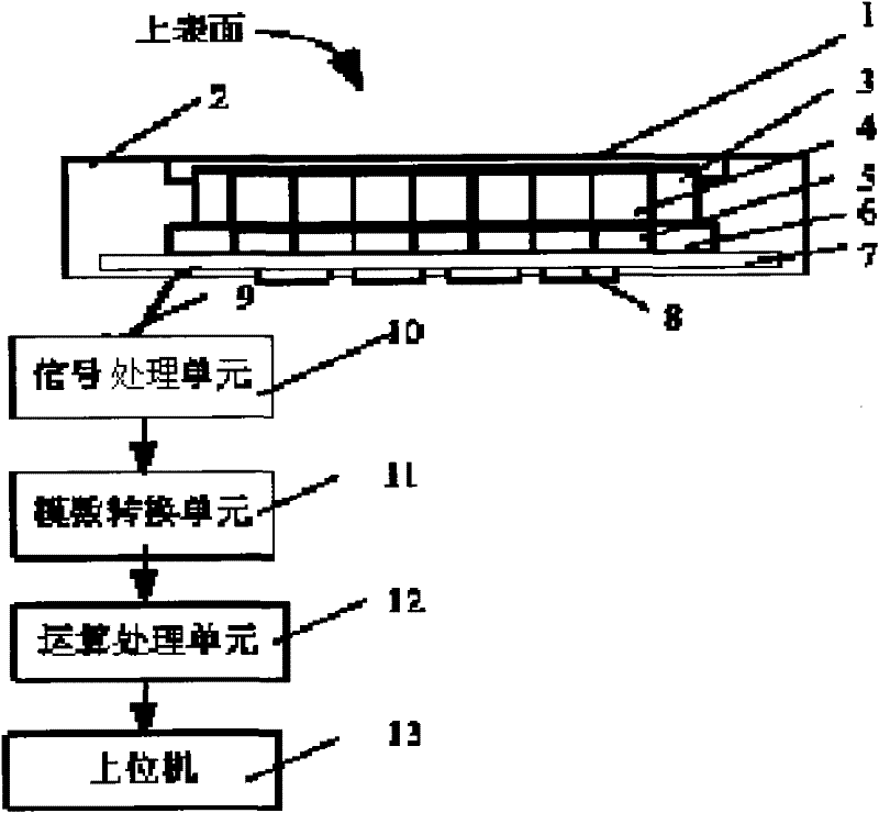
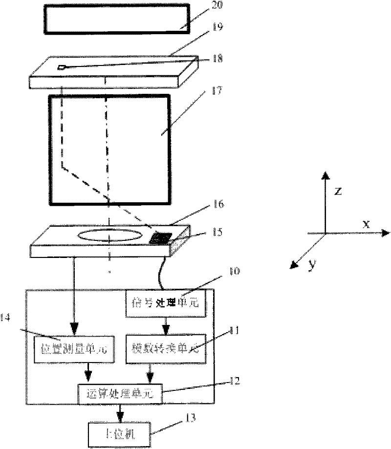
[0044] figure 1 Shown is a schematic structural view of the mask alignment surface shape detection device according to the present invention. As can be seen from the figure, the mask alignment surface detection device of the present invention includes a surface detection mark 1, a reference plate 2, an optical support 3, an optical filter 4, a surface photodiode 5, a spacer 6, a printed circuit Board 7 , amplifier 8 , signal output cable 9 , signal processing unit 10 , analog-to-digital conversion unit 11 , arithmetic processing unit 12 , and host computer 13 .

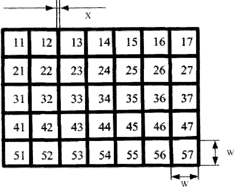
[0045]The surface detection mark 1 includes mult...


PUM


Abstract

The invention discloses a mask alignment surface shape detection device for a DUV (deep ultra violet) photolithographic device. The mask alignment surface shape detection device comprises surface shape detection marks, an optical filter, a surface shape silicon photoelectric diode, an amplifier, a signal processing element, an analogue to digital conversion element, an operation processing element and an upper computer, wherein the surface shape detection marks include a plurality of independent detection marks; the optical filter comprises a plurality of optical filter units for converting DUV into visible light; the surface shape silicon photoelectric diode comprises a plurality of independent units; the amplifier comprises a plurality of paths of amplifier units; the signal processing element comprises a plurality of signal processing units; and the analogue to digital conversion unit comprises a plurality of analogue to digital conversion units for performing analogue to digital conversion on analogue signals output by corresponding signal processing units. The surface shape detection device comprises a plurality of detection units, and each detection unit is provided with onecorresponding detection mark, one optical filter unit, one silicon photoelectric diode unit, one amplifier unit, one signal processing unit and one analogue to digital conversion unit.

Description

technical field [0001] The invention relates to the field of photolithography, in particular to a mask alignment surface detection device for a DUV photolithography device. Background technique [0002] The lithography machine belongs to a kind of key equipment on the process line of chip manufacturing. Its principle is to use the projection lens to illuminate the mask plate through the illumination source, and expose the pattern on the mask to the designated position on the silicon wafer. In order to accurately expose the pattern on the mask to the specified position, it is necessary to be equipped with a mask alignment system. The mask alignment system uses detectors on the silicon wafer to detect the imaging of the mask mark on the mask to obtain the imaging position. The positional relationship between the mask and the silicon wafer is achieved through mask alignment and silicon wafer alignment. [0003] The number of detection units of the existing detection device fo...

Claims


Application Information

Patent Timeline
Patent Type & Authority Applications(China)
IPC IPC(8): G03F7/20G03F9/00
Inventor 王海江唐文力李运锋程鹏陈振飞宋海军韦学志胡明辉
Owner SHANGHAI MICRO ELECTRONICS EQUIP (GRP) CO LTD
Why Eureka
Try Eureka