Nonvolatile charge capture type storage device, preparation method thereof and application

A storage device, charge capture technology, applied in static memory, read-only memory, semiconductor/solid-state device manufacturing, etc., can solve the problems of energy cost and less research on nanocrystals

Inactive Publication Date: 2013-08-28
NANJING UNIV
View PDF3 Cites 0 Cited by
  • Summary
  • Abstract
  • Description
  • Claims
  • Application Information

AI Technical Summary

Problems solved by technology

However, many researchers spend most of their energy on the preparation of metal nanocrystals and semiconductor nanocrystals for storage devices, and there is less research on other forms of nanocrystals

Method used


Image

  • Nonvolatile charge capture type storage device, preparation method thereof and application
  • Nonvolatile charge capture type storage device, preparation method thereof and application
  • Nonvolatile charge capture type storage device, preparation method thereof and application

Examples


Embodiment 1

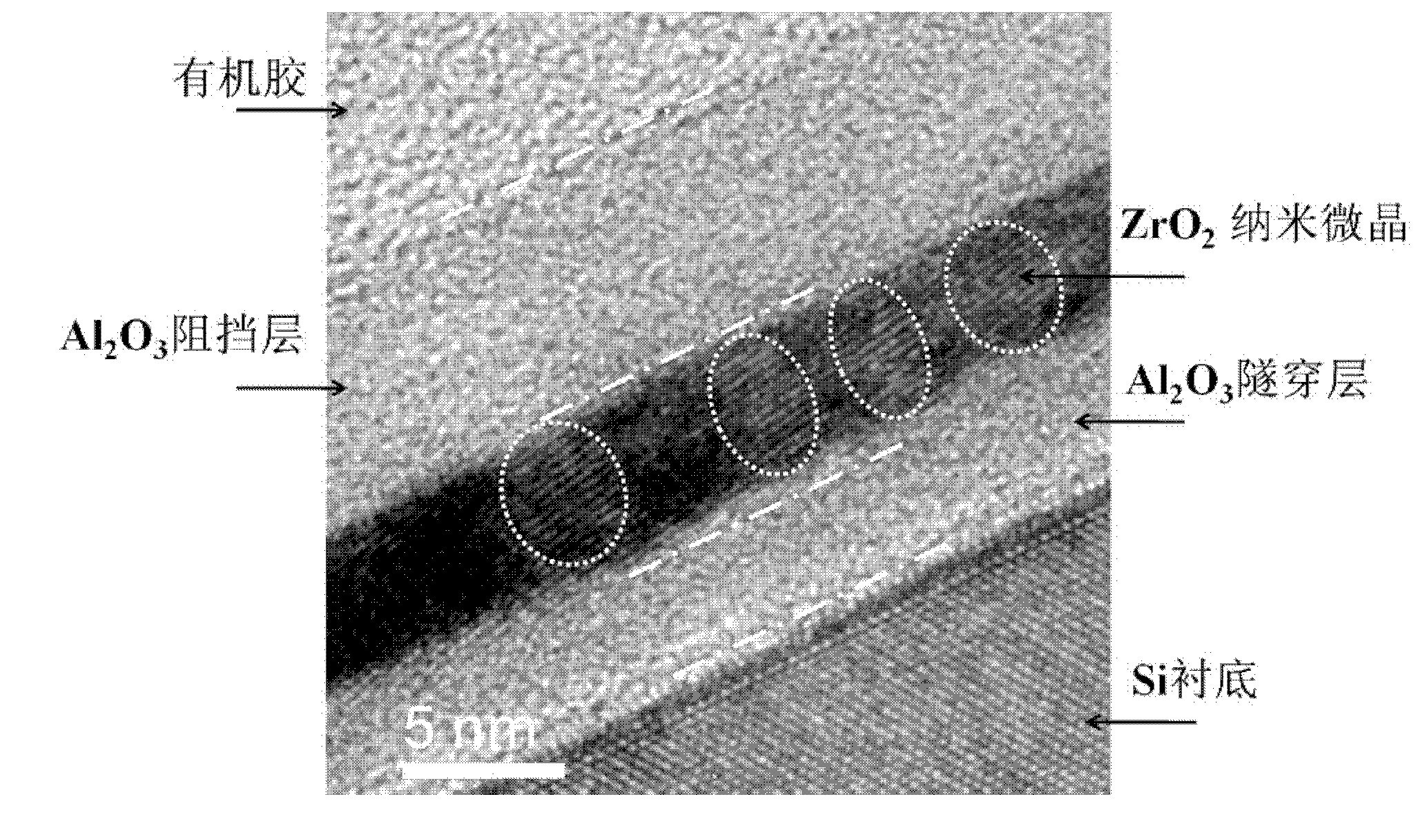
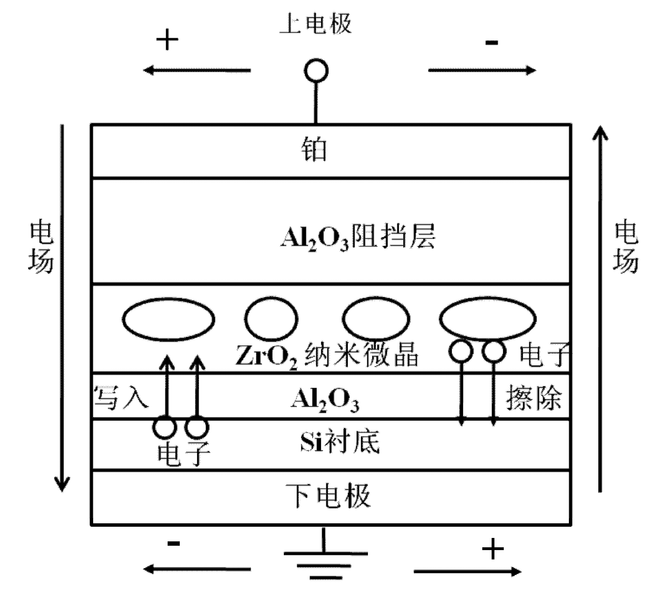
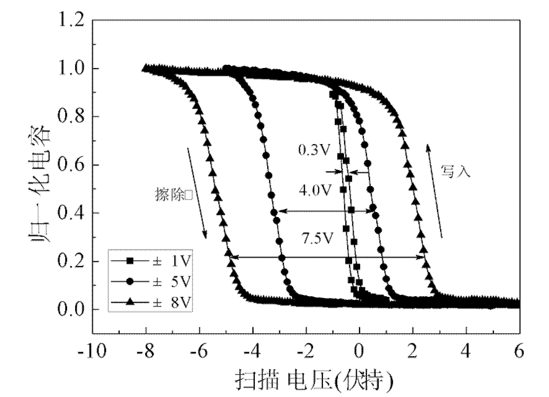
[0034] Embodiment 1: Based on Si substrate, ZrO 2 The preparation process of the nano-microcrystalline-based nonvolatile charge-trapping memory device is as follows:

[0035] (a) Put the Si substrate into an appropriate amount of acetone, ultrasonically clean it, and then ultrasonically clean it with deionized water to rinse off the remaining impurities on the surface of the substrate. Then the substrate is soaked in hydrofluoric acid to remove surface oxides, then ultrasonically cleaned with deionized water, dried with high-purity nitrogen, and then placed in an atomic layer chemical vapor deposition chamber for thin film deposition.

[0036] (b) Al(CH 3 ) 3 As a metal source, ozone is a source of oxygen. Al(CH 3 ) 3 With the nitrogen gas entering the cavity, it reacts with the surface of the hydroxyl-terminated silicon substrate and reaches saturation, and then the oxygen source is brought into the cavity by the nitrogen gas to react with the metal source to form Al 2 ...


PUM

PropertyMeasurementUnit
thicknessaaaaaaaaaa

Abstract

A non-volatile charge capture storage device, a method for preparing the same and an application thereof. The preparation method is simple to operate and easy to control, and the nano-microcrystal acting as a storage medium in the obtained storage device is evenly distributed. The preparation method includes the steps of: a) forming a tunneling layer on the substrate surface; b) forming a (ZrO2)x(M)1-x thin film with homogeneous composition acting as a storage layer on the tunneling layer, wherein l > x > 0.5, M is SiO2 or Al2O3; c) forming a barrier layer on the storage layer; d) and annealing the above prepared sample so as to precipitate the nano-microcrystal ZrO2 from the storage layer to act as the storage medium. By way of high temperature annealing processing, the nano-microcrystal ZrO2 is precipitated from the parent phase of the storage layer, thereby realizing the effect of nano-microcrystal storage. The nano-microcrystal acting as the storage medium obtained in the method is evenly distributed in the non-crystal parent phase.

Description

technical field [0001] The invention relates to a nonvolatile charge trapping memory device, its preparation method and application. Background technique [0002] For decades, the development of integrated circuits has basically followed the Moore's Law predicted by Dr. Gordon E. Moore, one of the founders of Intel Corporation, in 1964: 12 to 18 months doubles, feature size shrinks times. As the feature size of devices becomes smaller and smaller, traditional floating-gate non-volatile semiconductor memory devices face serious leakage problems. The size of the tunneling layer in the floating gate memory device is continuously reduced, so that a single defect will cause all the charges stored in the polysilicon floating gate to be lost. To solve this difficult problem, polysilicon-oxide-nitride-oxide-silicon (SONOS) type semiconductor memory devices have been extensively studied. In such devices, electrons are captured by the Si 3 N 4 A discrete trap capture in the sto...

Claims


Application Information

Patent Timeline
Patent Type & Authority Patents(China)
IPC IPC(8): H01L21/334C23C14/08C23C14/28H01L29/04H01L29/12H01L29/76
CPCH01L29/513B82Y10/00B82Y40/00C23C14/083C23C14/14C23C14/28C23C14/35C23C14/5806C23C16/0227C23C16/403C23C28/042G11C16/0475H01L29/40114H01L29/4234
Inventor 汤振杰夏奕东殷江刘治国
Owner NANJING UNIV
Why Eureka
Try Eureka