Preparation method of Through-Silicon-Via back coupling end

A technology for through-silicon vias and connection ends, which is applied in the field of preparation of back connection ends of through-silicon vias. Implementation and Yield Effects

Active Publication Date: 2011-10-05
NAT CENT FOR ADVANCED PACKAGING
View PDF4 Cites 7 Cited by
  • Summary
  • Abstract
  • Description
  • Claims
  • Application Information

AI Technical Summary

Problems solved by technology

[0007] In view of this, the main purpose of the present invention is to propose a method for preparing the connection end on the back of the through-silicon via, so as to solve the problem that in the prior art, when the back of the chip includes rewiring layer processing and other processes, there is a high tem

Method used


Image

  • Preparation method of Through-Silicon-Via back coupling end
  • Preparation method of Through-Silicon-Via back coupling end
  • Preparation method of Through-Silicon-Via back coupling end

Examples


preparation example Construction

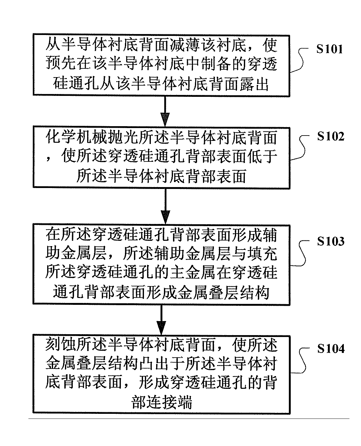
[0035] Such as figure 1 as shown, figure 1 It is a flowchart of a method for preparing the back connection end of a TSV provided by the present invention, and the method includes:

[0036] Step S101, thinning the semiconductor substrate from the back of the semiconductor substrate, so that the TSVs prepared in the semiconductor substrate in advance are exposed from the back of the semiconductor substrate;

[0037] Step S102, chemical mechanical polishing the back surface of the semiconductor substrate, so that the back surface of the TSV is lower than the back surface of the semiconductor substrate;

[0038] Step S103, forming an auxiliary metal layer on the back surface of the TSV, the auxiliary metal layer and the main metal filling the TSV form a metal stack structure on the back surface of the TSV;

[0039] Step S104, etching the back surface of the semiconductor substrate to make the metal stacked structure protrude from the back surface of the semiconductor substrate t...

Embodiment

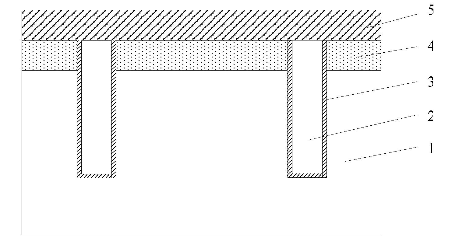
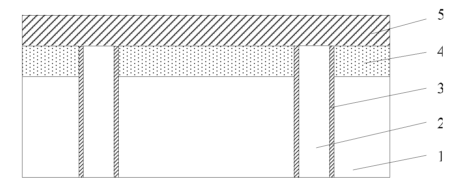
[0042] This embodiment will take the complete preparation process of the back connection end of the TSV as an example for illustration. The semiconductor substrate used in this embodiment is as figure 2 shown. The through-silicon via has been prepared on the semiconductor substrate 1, and the material for filling the through-silicon via includes the main metal 2 and the sidewall isolation layer material 3, and the semiconductor substrate 1 is also completed The processing of the semiconductor device layer 4 and the interconnection layer 5 is completed. The main metal is copper or tungsten, and the isolation layer material is one or more combinations of the following materials: silicon oxide, silicon nitride, titanium, tantalum, titanium nitride, tantalum nitride, ruthenium. The subsequent preparation of the back connection end of the TSV includes the following steps:

[0043] Step 1: Thinning the semiconductor substrate 1 on the back side, so that the TSV (combination of 2...


PUM


Abstract

The invention discloses a preparation method of a Through-Silicon-Via (TSV) back coupling end. The method comprises thinning a semiconductor substrate from the back side of the semiconductor substrate to make a TSV prepared in the semiconductor substrate in advance expose from the back of the semiconductor substrate, carrying out a chemically mechanical polishing towards the back of the semiconductor substrate to make the back surface of the TSV lower than that of the semiconductor substrate, forming an auxiliary metal layer on the back surface of the TSV, wherein the auxiliary metal layer and the main metal filling the TSV form a metal lamination composition on the back surface of the TSV, etching the back of the semiconductor substrate to make the metal lamination composition protrude from the back surface of the semiconductor substrate so as to form the TSV back coupling end. According to the invention, a recess effect of the chemically mechanical polishing technology is utilized to superpose the auxiliary metal layer on the back surface of the TSV in the modes of free mask and low temperature and the feasibility and yield of using the TSV to realize stacking and integration of multilayer microelectronic chips are improved.

Description

technical field [0001] The invention relates to the technical field of semiconductor preparation and three-dimensional integration, in particular to a method for preparing a connection end at the back of a through-silicon hole. Background technique [0002] Three-dimensional integration technology uses Through-Silicon-Via (TSV) to realize the communication of multi-layer chips, which can effectively shorten the length of interconnection lines between chips and provide heterogeneous integration capabilities. It is an important direction for the development of microelectronics technology. . To achieve three-dimensional integration, three key technologies are required: preparation of through-silicon vias, chip thinning and transfer, and stacking and bonding. It is one of the core technologies to achieve three-dimensional integration to obtain an effective electrical connection between the back of the through-silicon via and another layer of chips. At present, it mainly relies ...

Claims


Application Information

Patent Timeline
IPC IPC(8): H01L21/768
Inventor 宋崇申于大全
Owner NAT CENT FOR ADVANCED PACKAGING
Why Eureka
Try Eureka