Flexible substrate used in luminescent device and preparation method thereof

A technology for light-emitting devices and substrates, which is applied in the manufacture of semiconductor/solid-state devices, electric solid-state devices, semiconductor devices, etc., and can solve the problems of poor bonding force between carbon nanotubes and flexible substrates, and poor surface flatness of thin-layer carbon nanotubes. , to achieve high visible light transmittance, enhanced luminous intensity, and improved visible light transmittance

Inactive Publication Date: 2011-10-05
UNIV OF ELECTRONIC SCI & TECH OF CHINA
View PDF2 Cites 6 Cited by
  • Summary
  • Abstract
  • Description
  • Claims
  • Application Information

AI Technical Summary

Problems solved by technology

[0008] The technical problem to be solved by the present invention is how to provide a substrate for flexible light-emitting devices and its preparation method. The substrate solves the problems of poor surface flatnes

Method used


Image

  • Flexible substrate used in luminescent device and preparation method thereof
  • Flexible substrate used in luminescent device and preparation method thereof
  • Flexible substrate used in luminescent device and preparation method thereof

Examples


Embodiment 1

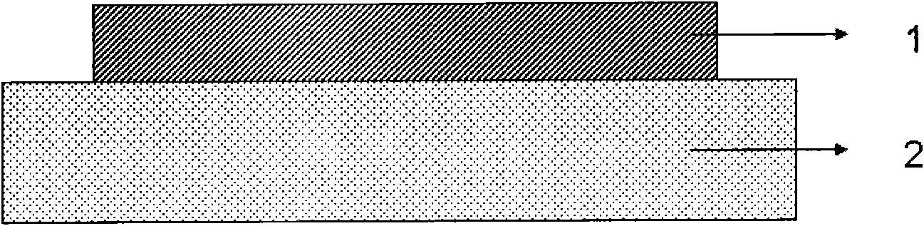
[0074] Such as figure 1 As shown in the substrate structure, the flexible substrate 1 adopts a UV-curable silicone adhesive, and the UV-curable silicone adhesive includes 95% photosensitive polysiloxane, 2% photoinitiator and 3% diluted agent and auxiliary agent, the conductive layer 2 adopts carbon nanotubes, and the voids of the carbon nanotube layer are filled with inorganic luminescent nanoparticles, the size of the inorganic luminescent nanoparticles is 20 nanometers, and the thickness of the carbon nanotube layer is 80 nanometers.

[0075] The preparation method is as follows:

[0076] ① Clean the silicon substrate whose surface roughness is less than 1nm, and dry it with dry nitrogen after cleaning;

[0077] ② Disperse carbon nanotubes evenly in a solvent, and prepare a carbon nanotube layer on a clean silicon substrate by spin coating. The rotation speed of spin coating is 4000 rpm, the duration is 60 seconds, and the film thickness is about 80 nanometers;

[0078] ③...

Embodiment 2

[0083] Such as figure 1 As shown in the substrate structure, the flexible substrate 1 adopts a UV-curable silicone adhesive, and the UV-curable silicone adhesive includes 92% photosensitive polysiloxane, 5% photoinitiator and 3% diluted The conductive layer 2 adopts carbon nanotubes, and the voids of the carbon nanotube layer are filled with inorganic luminescent nanoparticles. The size of the inorganic luminescent nanoparticles is 15 nanometers, and the thickness of the carbon nanotube layer is 70 nanometers.

[0084] The preparation method is similar to Example 1.

Embodiment 3

[0086] Such as figure 1 As shown in the substrate structure, the flexible substrate 1 adopts UV-curable silicone adhesive, which includes 92% photosensitive polysiloxane, 2% photoinitiator and 6% diluted The conductive layer 2 adopts carbon nanotubes, and the voids of the carbon nanotube layer are filled with inorganic luminescent nanoparticles. The size of the inorganic luminescent nanoparticles is 10 nanometers, and the thickness of the carbon nanotube layer is 60 nanometers.

[0087] The preparation method is similar to Example 1.


PUM

PropertyMeasurementUnit
Sizeaaaaaaaaaa
Thicknessaaaaaaaaaa
Surface roughnessaaaaaaaaaa

Abstract

The invention discloses a flexible substrate used in a luminescent device. The substrate comprises a flexible substrate and a conducting layer. The flexible substrate and the conducting layer are formed in one of the following two ways: (1) the flexible substrate is organosilicon adhesive which is solidified by ultraviolet light and the conducting layer is thin layer carbon nanotube, wherein the gap of the thin layer carbon nanotube is filled with inorganic luminescence nanometer particle; (2) the flexible substrate is organosilicon adhesive which is solidified by ultraviolet light and doped with inorganic luminescence nanometer particle, and the conducting layer is thin layer carbon nanotube, wherein the gap of the thin layer carbon nanotube is filled with organosilicon adhesive which is solidified by ultraviolet light and doped with inorganic luminescence nanometer particle. According to the substrate provided in the invention, the problems of the poor surface flatness of the thin layer carbon nanotube and the poor bonding force between the carbon nanotube and the flexible substrate are solved, and the conductivity of the conducting layer and the obstructing capability to water and oxygen of the substrate are improved.

Description

technical field [0001] The invention relates to the technical field of organic optoelectronics, in particular to a substrate for a flexible light-emitting device and a preparation method thereof. Background technique [0002] Optoelectronics technology is a rapidly developing industry with high technological content after microelectronics technology. With the rapid development of optoelectronic technology, optoelectronic products such as solar cells, optical image sensors, flat panel displays, and thin film transistors have gradually matured, and they have greatly improved people's lives. At the same time, the wide application of optoelectronic information technology in various fields of social life has also created a huge growing market. Developed countries regard the optoelectronic information industry as one of the key development areas, and the competition in the optoelectronic information field is unfolding worldwide. [0003] Optoelectronics technology is a rapidly d...

Claims


Application Information

Patent Timeline
IPC IPC(8): H01L51/52H01L51/54C09J183/04H01L51/56
Inventor 于军胜李璐王婉蒋亚东
Owner UNIV OF ELECTRONIC SCI & TECH OF CHINA
Why Eureka
Try Eureka