

Printing method of microform graph-text
A printing method and micro-text technology, applied in the field of printing, can solve the problems such as the inability of printing technology to be realized, and achieve the effect of solving technical problems and broad application prospects.
- Summary
- Abstract
- Description
- Claims
- Application Information
AI Technical Summary
Problems solved by technology
Method used
Image

Examples
preparation example Construction
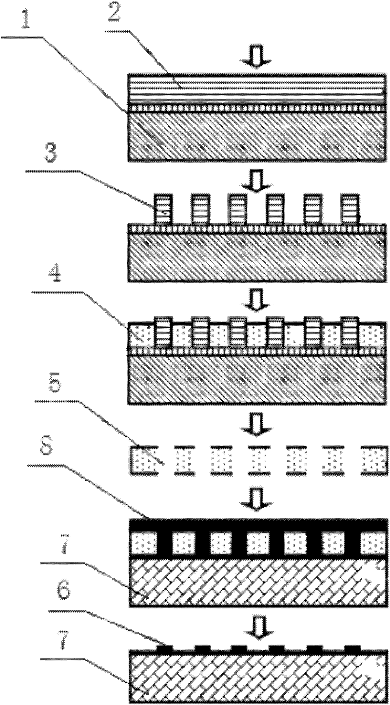
[0035] The preparation method of the described nickel plate 10 with the hollow micro-graphic structure 5 comprises the following steps:
[0036] (1) Coating a polymer material on the conductive substrate 1 to obtain a conductive substrate 1 with a polymer coating 2;
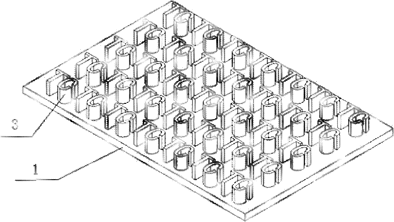
[0037] (2) Using micromachining technology to form a micrographic structure 3 on the polymer coating 2 to obtain a conductive substrate 1 with an island micrographic structure 2. For the micrographic structure 3, see figure 2 , wherein, the micro-text, such as "TC" in the figure, is an isolated protrusion on the conductive substrate 1, and the conductive substrate 1 in the place where there is no micro-text structure is exposed;
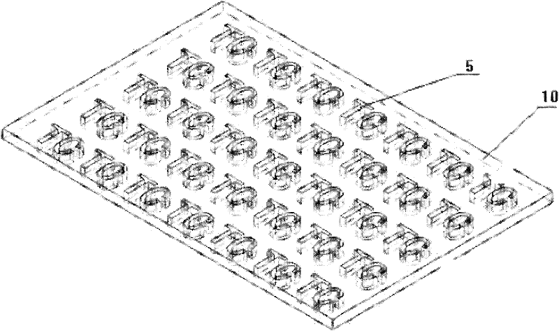
[0038] (3) The conductive substrate with the island micro-text structure 3 obtained in step (2) is placed in the electrolyte, and micro-electroformed nickel is carried out. In the gaps of the island micro-text structure, a nickel layer 4 is formed and electroformed. After the end, the...
Embodiment 1
[0041] (1) The substrate is made of silicon wafers. The silicon wafers are first cleaned and baked in an oven at 180°C for 4 hours to remove surface water molecules. A layer of titanium metal film with a thickness of 2um is formed on the surface of the silicon wafers by a sputtering machine. , coating a photoresist with a thickness of 40 um on the surface of the metal titanium film, and drying to obtain a conductive substrate with a photoresist coating. The photoresist is the SU-8 series produced by MicroChem Corp. of the United States.
[0042] (2) Adopt the method for mask photolithography, form micrographic structure on photoresist coating: used mask plate such as Figure 4 As shown, it is a quartz chromium plate. For the preparation method of the mask plate, you can refer to the method reported in the literature of Wang Weijun et al. Micron lines, the text line width is 8 microns. The part of the miniature characters is black, representing opacity, and the rest is white, ...
Embodiment 2
[0055] Using the same method as in Example 1, wherein, in step (3), the conductive substrate with the isolated island micro-graphic structure obtained in step (2) is placed in the electrolyte, the conductive substrate is the cathode, and nickel is the anode, and the Micro-electroforming nickel forms nickel pillars in the gaps of the isolated island micro-graphic structure, and the height of the nickel pillars is less than the thickness of the photoresist layer and is 50% of the thickness of the photoresist layer.
[0056] Electroforming conditions are as follows: pH value: 5.1; temperature: 50°C.
[0057] Cover the surface of the printing material 7 with the nickel plate 10 having the hollowed-out micro-text structure 5, and use it as a printing plate, and the printing material with micro-text can be obtained by scraping printing.
[0058]Among them, the thickness of the nickel plate with hollowed-out micrographics is 20 microns, and the thinnest seam is 8 microns.
PUM
| Property | Measurement | Unit |
|---|---|---|
| Thickness | aaaaa | aaaaa |
Abstract
Description
Claims
Application Information