Ultraviolet light curing device and alarm method thereof

A technology of ultraviolet light and equipment, which is applied in microlithography exposure equipment, alarms, exposure devices for photolithography, etc., can solve the problems of high scrap rate of substrates, achieve high alarm accuracy, avoid production loss, and troubleshoot in a timely manner Effect

Active Publication Date: 2011-11-02
SHANGHAI HUAHONG GRACE SEMICON MFG CORP
View PDF6 Cites 4 Cited by
  • Summary
  • Abstract
  • Description
  • Claims
  • Application Information

AI Technical Summary

Problems solved by technology

[0004] In the existing photolithography process, the photoresist or photoresist pattern is usually baked one or more times (soft baking or hard baking) to remove the moisture of the photoresist or photoresist pattern. UV light curing equipment is usually used for baking, but the substrate scrap rate after baking with existing UV light curing equipment is high

Method used


Image

  • Ultraviolet light curing device and alarm method thereof
  • Ultraviolet light curing device and alarm method thereof
  • Ultraviolet light curing device and alarm method thereof

Examples


Embodiment Construction

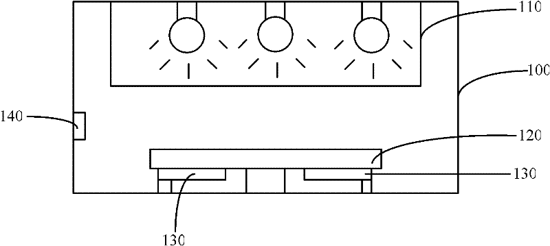
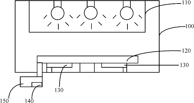
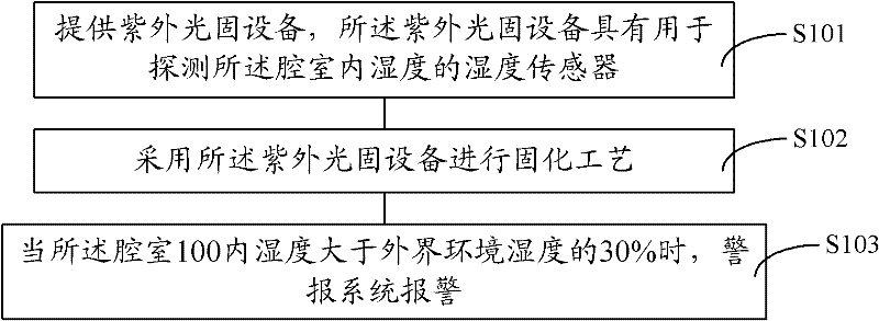
[0018] The inventors of the present invention have found in actual work that the scrap rate of substrates baked by existing ultraviolet light curing equipment is high. The inventors further analyzed the scrapped substrates and found that all scrapped substrates have water stains. The substrate was contaminated during the photocuring process due to water leakage.

[0019] For this reason, the inventors of the present invention have further researched and found that the reason for the water leakage of the UV curing equipment and the formation of water stains on the substrate is that during the UV curing process, the substrate is placed on the surface of the UV curing equipment. substrate carrier (wafer chuck), and when UV curing is performed, the water cooling system of the substrate carrier cools the substrate through water cooling. When the cooling system leaks, the cooling water will spread to the The substrate is placed on the tray, causing the substrate to be polluted by wa...


PUM


Abstract

The invention provides an ultraviolet light curing device and an alarm method thereof, wherein the ultraviolet light curing device comprises a chamber, an ultraviolet light generating device, a substrate bearing disc, a water cooling device and a humidity sensor, wherein the ultraviolet light generating device is arranged in the chamber; the substrate bearing disc is arranged opposite to the ultraviolet light generating device; the water cooling device is arranged at the bottom of the substrate bearing disc; the humidity sensor is used for detecting the humidity in the chamber, and the humidity sensor gives out an alarm when the humidity in the chamber is greater than a set value. The ultraviolet light curing device and the alarm method thereof provided by the invention can be used for avoiding the production losses in a light curing process in batches and further has the advantages of high alarm accuracy, large alarm range and timely trouble shooting.

Description

technical field [0001] The invention relates to the field of semiconductor manufacturing equipment, in particular to ultraviolet light curing equipment and an alarm method for ultraviolet light curing equipment. Background technique [0002] Photolithography is one of the most important process steps in semiconductor manufacturing. The main function is to copy the pattern on the mask plate to the silicon wafer to prepare for the next semiconductor process, such as etching or ion implantation; the cost of photolithography is about 1 / 3 of the entire silicon wafer manufacturing process, which consumes The time accounts for about 40-60% of the entire wafer process. [0003] A photolithography process is disclosed in the Chinese patent with the publication number CN 101592866A, which specifically includes: providing a substrate to be photoetched; cleaning and drying the substrate; spin-coating the dried substrate for photolithography glue to form a photoresist layer; soft-bakin...

Claims


Application Information

Patent Timeline
IPC IPC(8): G03F7/20G08B21/20
Inventor 王旭东施海铭巴文林徐立
Owner SHANGHAI HUAHONG GRACE SEMICON MFG CORP
Why Eureka
Try Eureka