Preparation method of single crystal silicon texture surface structure

A monocrystalline silicon and suede technology, which is applied in the field of solar energy applications, can solve the problems of restricting production capacity, slow formation speed of suede surface, and limitation of battery efficiency, etc., and achieve the effects of increasing production capacity, saving process time, and fast forming speed

Active Publication Date: 2011-11-09
BEIJING NAURA MICROELECTRONICS EQUIP CO LTD
View PDF2 Cites 22 Cited by
  • Summary
  • Abstract
  • Description
  • Claims
  • Application Information

AI Technical Summary

Problems solved by technology

[0004] However, in the process of realizing the preparation of the above-mentioned textured structure, the inventors found that there are at least the following problems in the prior art: although the textured structure prepared by the chemical corrosion method reduces the reflection loss of sunlight relative to the smooth structure, due to The size of the suede pyramid prepared by this method is usually in the order of 3-15 microns (um), which i...

Method used


Image

  • Preparation method of single crystal silicon texture surface structure
  • Preparation method of single crystal silicon texture surface structure
  • Preparation method of single crystal silicon texture surface structure

Examples


preparation example Construction

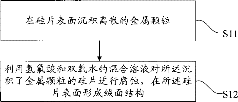
[0022] The preparation method of the suede that the embodiment of the present invention provides, such as image 3 The flowchart shown includes:

[0023] S11, depositing discrete metal particles on the surface of the silicon wafer;

[0024] S12, using a mixed solution of hydrofluoric acid and hydrogen peroxide to etch the silicon wafer on which the metal particles are deposited, to form a textured structure on the surface of the silicon wafer.

[0025] The suede preparation method provided in the embodiment of the present invention may be called a metal-catalyzed silicon corrosion method. At present, in the field of scientific research, the metal-catalyzed silicon etching method is mainly used to prepare silicon nanostructures, such as quantum dots, porous silicon, nanowires, etc. Its main principle is that in the environment of strong oxidizing HF acid solution, metal particles are used as catalysts to oxidize the silicon surface in contact with the metal particles through ...

Embodiment 1

[0044] The preparation method of the suede that present embodiment provides, as Figure 5 The flow chart shown includes the following steps:

[0045] S21, performing standard cleaning on the silicon wafer;

[0046] S21, using the chemical plating method, immerse the silicon wafer in HF and silver nitrate (AgNO 3 ) in the mixed solution, depositing discrete Ag particles on the surface of the silicon wafer.

[0047] This step is carried out at room temperature, the reaction time is 1min, the HF and AgNO 3 In the mixed solution, the concentration of HF is 10%, AgNO 3 The concentration is 0.01~0.03Mol / L. After this step, discrete and evenly distributed Ag particles will be deposited on the surface of the silicon wafer. After this step, the topography of the silicon wafer surface is as follows: Image 6 As shown, the white particles in the figure are deposited Ag particles. It can be seen from the figure that the deposited Ag particles are discrete, evenly distributed and com...


PUM

PropertyMeasurementUnit
Concentrationaaaaaaaaaa

Abstract

The invention provides a preparation method of a single crystal silicon texture surface structure, relates to the technical field of solar energy application, and is invented to effectively reduce reflection loss of incident light of a texture surface and to increase forming speed of a texture surface. The preparation method of a single crystal silicon texture surface comprises the following steps: depositing discrete metal particles on a silicon wafer surface; performing corrosion of the silicon wafer deposited with metal particles by a mixed solution of hydrofluoric acid and hydrogen peroxide so as to form a texture surface structure on the silicon wafer surface. The invention is applicable to the preparation process of solar cells.

Description

technical field [0001] The invention relates to the technical field of solar energy applications, in particular to a method for preparing a monocrystalline silicon textured structure. Background technique [0002] The preparation of the textured structure is a common process in the production process of crystalline silicon solar cells. The textured structure can effectively reduce the reflection loss of incident light on the surface of the silicon wafer, increase the utilization rate of light, and then improve the conversion efficiency of the cell. Such as figure 1 As shown, the typical structure of suede currently used is a suede pyramid structure. For a smooth silicon wafer, about 33% of the sunlight incident on the surface is reflected by the surface and cannot be absorbed by the battery. For the suede pyramid structure, due to the pyramid structure on the surface, the incident reflected light will be incident again to reduce the reflection loss. [0003] In the prior ...

Claims


Application Information

Patent Timeline
IPC IPC(8): C30B33/10C23F1/24C23F1/02
Inventor 肖青平
Owner BEIJING NAURA MICROELECTRONICS EQUIP CO LTD
Why Eureka
Try Eureka