Method and device for manufacturing liquid crystal display panel

A technology of liquid crystal display panels and manufacturing methods, applied in the direction of nonlinear optics, instruments, optics, etc., can solve the problems of large floor area, high production cost, and production line can only be stopped, so as to reduce floor space and production cost , the effect of improving production efficiency

Inactive Publication Date: 2011-11-09
TCL CHINA STAR OPTOELECTRONICS TECH CO LTD
View PDF6 Cites 15 Cited by
  • Summary
  • Abstract
  • Description
  • Claims
  • Application Information

AI Technical Summary

Problems solved by technology

[0005] Although the production process of the above-mentioned LCD liquid crystal display panel saves the unit time of producing the liquid crystal display panel, because the preparation time of the TFT substrate and the CF substrate are inconsistent, there must be a part of the production line in the idle state during the production process, and the liquid crystal display of the entire production line Plate production efficiency is not high
Especially in the case of a production line failure, the other corresponding production line can only be shut down, which greatly affects production efficiency
At the same time, the production line of liquid crystal display panels has high equipment costs and a large floor area, and the production of liquid crystal display panels with two production lines makes the production cost relatively high

Method used


Image

  • Method and device for manufacturing liquid crystal display panel
  • Method and device for manufacturing liquid crystal display panel
  • Method and device for manufacturing liquid crystal display panel

Examples


Embodiment Construction

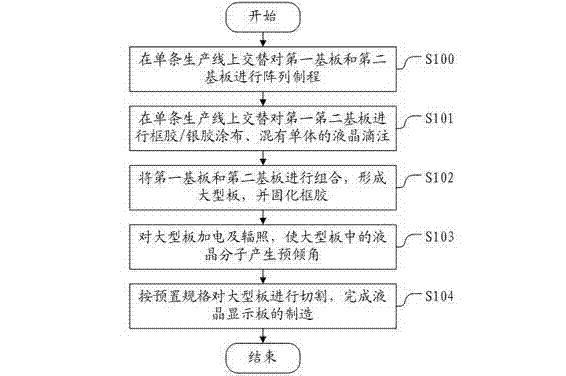
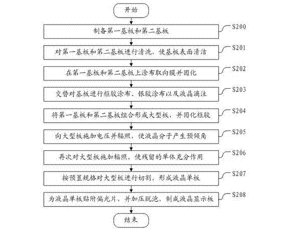
[0047] The method and device for manufacturing a liquid crystal display panel provided by the embodiments of the present invention can complete the production of a liquid crystal display panel on a single production line, avoiding an idle state in the production line of a liquid crystal display panel, and improving production efficiency. At the same time, the floor space occupied by the production line equipment of the liquid crystal display panel is reduced, and the production cost of the liquid crystal display panel is reduced.

[0048] The following will clearly and completely describe the technical solutions in the embodiments of the present invention with reference to the accompanying drawings in the embodiments of the present invention. Obviously, the described embodiments are only some, not all, embodiments of the present invention. Based on the embodiments of the present invention, all other embodiments obtained by persons of ordinary skill in the art without creative e...


PUM


Abstract

The embodiment of the invention discloses a method and device for manufacturing a liquid crystal display panel. The manufacturing method comprises the following steps of: alternately processing a first substrate and a second substrate on a single production line, completing array processing, frame glue coating, silver glue coating and monomer-mixed liquid crystal instilling on the first substrate and the second substrate, wherein the first substrate is a thin film field effect transistor (TFT) substrate, and the second substrate is a colour filter (CF) substrate; combining the first substrate with the second substrate to form a large panel, and curing the frame glue; carrying out power on and radiation on the large panel to cause liquid crystal molecules in the large panel to produce a pretilt angle; and cutting the large panel according to a preset specification so as to complete manufacturing of the liquid crystal display panel. By adopting the method and device for manufacturing the liquid crystal display panel, provided by the embodiment of the invention, production of the liquid crystal display panel can be completed on the single production line, an idle state of the production line of the liquid crystal display panel is avoided, production efficiency is improved, occupying area of equipment of the production line is reduced, and production cost of the liquid crystal display panel is reduced.

Description

technical field [0001] The invention relates to the field of production and manufacture of liquid crystal display panels, in particular to a method and device for manufacturing a liquid crystal display panel. Background technique [0002] Liquid crystal display, or LCD (Liquid Crystal Display), is a flat and ultra-thin display device. LCD is a display made of liquid crystal (LC, Liquid Crystal). Liquid crystals are organic compounds between solid and liquid. Under the action of the electric field, the liquid crystal molecules will rotate to change the light transmittance, thereby realizing multi-gray scale display. The changes in the arrangement of the liquid crystal molecules affect the changes in the light passing through them, and the changes in light can be expressed as changes in brightness and darkness through the action of polarizers. Through the control of the electric field, the liquid crystal display finally controls the light and dark changes of the light, so a...

Claims


Application Information

Patent Timeline
Patent Type & Authority Applications(China)
IPC IPC(8): G02F1/1333
CPCG02F1/1303G02F2001/1316G02F2001/133354G02F1/133351G02F1/133788G02F1/1333G02F1/1316G02F1/133354
Inventor 吴若杉陈虹瑞
Owner TCL CHINA STAR OPTOELECTRONICS TECH CO LTD
Why Eureka
Try Eureka