Manufacturing method of single intermetallic compound micro-interconnecting structure of flip chip

A flip-chip, interconnect structure technology, applied in metal processing equipment, manufacturing tools, welding equipment, etc., can solve problems such as failure, electronic products can not work, fracture, etc., to achieve improved creep resistance, excellent stability, The effect of improving reliable performance

Inactive Publication Date: 2011-11-16
HARBIN INST OF TECH
View PDF6 Cites 22 Cited by
  • Summary
  • Abstract
  • Description
  • Claims
  • Application Information

AI Technical Summary

Problems solved by technology

[0005] The purpose of the present invention is to provide a method for preparing a flip-chip single intermetallic compound micro-interconnection structure, to solve the problem that the flip-chip micro-interconnection solder joint is composed of chip metal pad-intermetallic compound-brazing alloy-intermetallic compound- Substrate metal pads, due to the different materials of so...

Method used


Image

  • Manufacturing method of single intermetallic compound micro-interconnecting structure of flip chip
  • Manufacturing method of single intermetallic compound micro-interconnecting structure of flip chip
  • Manufacturing method of single intermetallic compound micro-interconnecting structure of flip chip

Examples


specific Embodiment approach 1

[0019] Specific Embodiment 1: The method for preparing a flip-chip single intermetallic compound micro-interconnection structure in this embodiment is realized by the following steps:

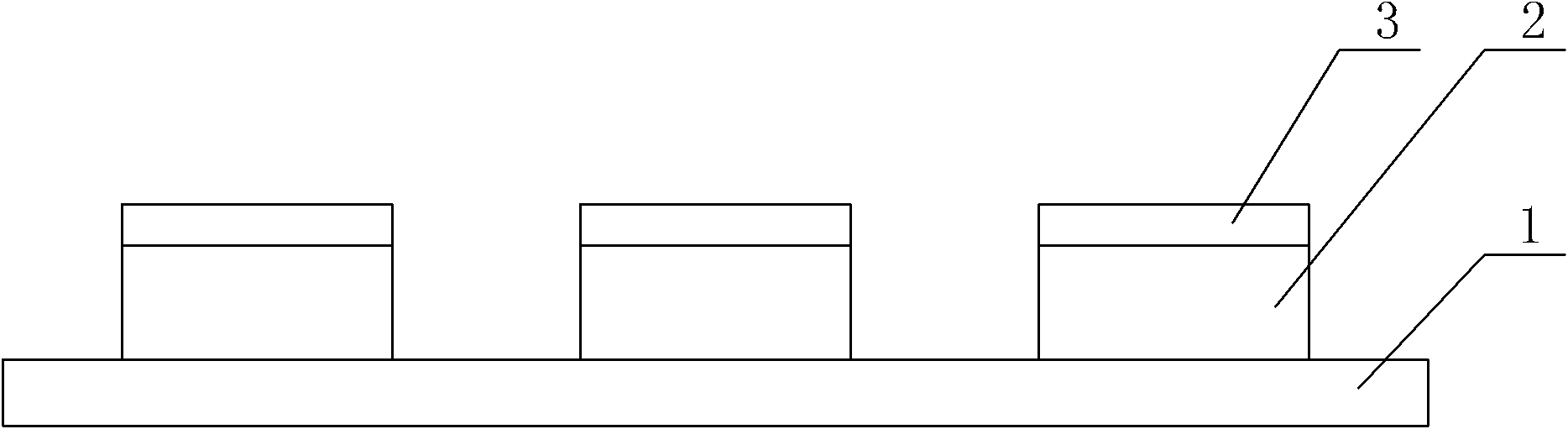
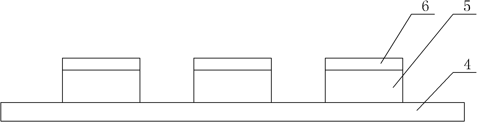
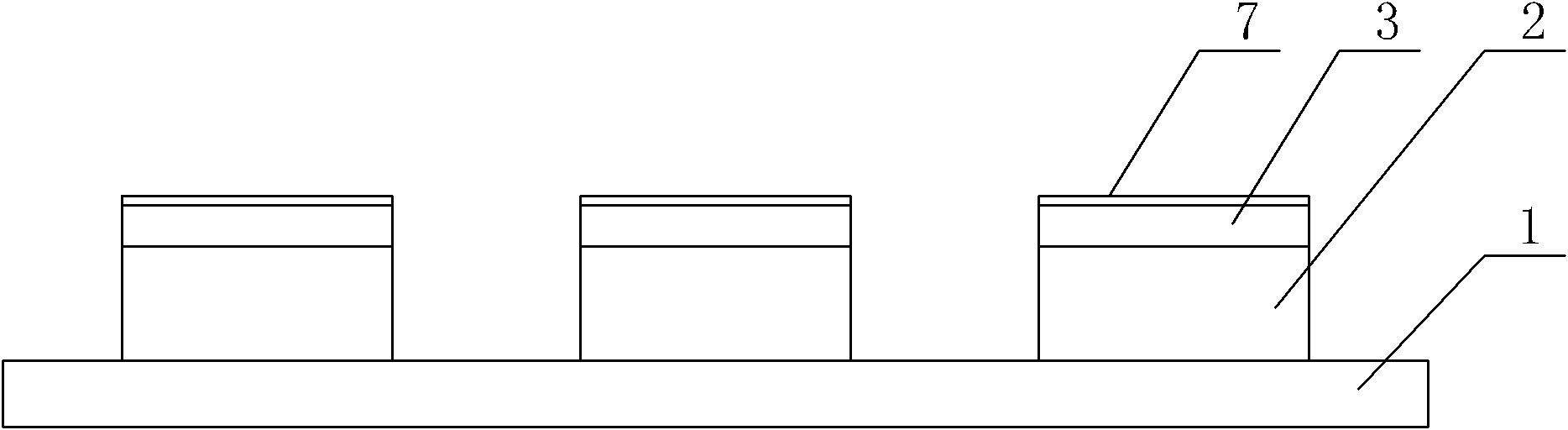
[0020] Step 1: prepare a chip metal base layer 2 on each metal surface on the chip 1, prepare a chip metal surface layer 3 on the horizontal plane of the chip metal base layer 2, and the chip metal base layer 2 is defined as a chip metal pad (see Figure 1a ); prepare substrate metal base layer 5 on each metal surface on substrate 4, prepare substrate metal surface layer 6 on the horizontal plane of described substrate metal base layer 5, and described substrate metal base layer 5 is defined as substrate metal pad (referring to Figure 1b ); the material of the chip metal pad and the material of the substrate metal pad are Cu, Au, Pd, Ag, Ni or Pt, and the material of the chip metal pad is the same as that of the substrate metal pad, and the chip The metal surface layer 3 and the substrate metal...

specific Embodiment approach 2

[0025] Embodiment 2: In step 1 of this embodiment, the metal pads of the chip and the metal pads of the substrate are in the shape of a cylinder or a cube, and the diameter of the metal pad of the chip in the shape of the cylinder is the same as the metal pad of the substrate in the shape of the cylinder. The diameters of the bonding pads are both 20-1000 μm; the side lengths of the cube-shaped chip metal pads and the side lengths of the cube-shaped chip metal pads are both 20-1000 μm. It can meet the requirements of different solder joint sizes in electronic packaging. Other method steps are the same as those in the first embodiment.

specific Embodiment approach 3

[0026] Embodiment 3: In step 1 of this embodiment, the ratio of the thickness of the metal pad of the substrate to the thickness of the metal surface layer of the substrate ranges from 5:1 to 10:1. In order to generate single intermetallic compound solder joints. Other method steps are the same as those in the first or second embodiment.


PUM

PropertyMeasurementUnit
Diameteraaaaaaaaaa
Thicknessaaaaaaaaaa
Thicknessaaaaaaaaaa

Abstract

The invention discloses a manufacturing method of a single intermetallic compound micro-interconnecting structure of a flip chip, relating to the manufacturing method of an intermetallic compound micro-interconnecting structure of the flip chip and aiming at solving the problem that micro-interconnection welding spots of the flip chip fracture at connecting interfaces among brazing solder alloys, intermetallic compounds and metallic bonding pads. The technical scheme I comprises the following steps of: manufacturing a chip metallic basic layer (a chip metallic bonding pad) and a surface layer on a metallic surface of the chip, and manufacturing a substrate metallic basic layer (a substrate metallic bonding pad) and a surface layer on a metallic surface of a substrate, wherein the chip and the substrate metallic surface are made of pure Sn; coating a soldering flux on the metallic surface of the chip and the metallic surface of the substrate; and inverting the chip to ensure that the chip metallic bonding pad corresponds to the substrate metallic bonding pad, pressing, heating, cooling, and forming the intermetallic compound micro-interconnecting structure of the flip chip. The technical scheme II is different from the technical scheme I in the following steps of: coating the soldering flux on the metallic basic layer of the chip and the metallic basic layer of the substrate and inverting the chip, wherein the metallic basic layer of the chip is in contact with the metallic bonding pad of the substrate by a Sn foil. The single intermetallic compound micro-interconnecting structure is applied to an electronic packaging structure.

Description

technical field [0001] The invention relates to a method for preparing a flip-chip intermetallic compound micro-interconnection structure, which belongs to the field of electronic package structure design and manufacture. Background technique [0002] Flip-chip technology is to mount the chip directly on the surface of the substrate in an upside-down manner. This chip interconnection method can provide higher input / output connection density. The area occupied by the flip-chip is almost the same as the chip size. Small and thin encapsulation. [0003] While electronic products are developing in the direction of miniaturization and multi-function, higher requirements are also put forward for their reliability. Micro-interconnection solder joints, as a bridge between the chip and the substrate for electrical and mechanical connections, have a crucial impact on the reliability of electronic products. [0004] At present, flip-chip micro-interconnection solder joints are formed...

Claims


Application Information

Patent Timeline
IPC IPC(8): H01L21/603H01L23/00H01L23/488B23K31/02
CPCH01L2224/16503H01L2224/8181
Inventor 刘威王春青田艳红孔令超
Owner HARBIN INST OF TECH
Why Eureka
Try Eureka