Silicon-on-insulator (SOI) substrate structure and device

An insulator and silicon substrate technology, applied in the field of silicon substrate structures and devices, can solve problems such as increased power consumption, loss of BOX15, increased capacitance, etc., and achieve the effects of increased operating speed, reduced procedures, and reduced power consumption

Inactive Publication Date: 2011-11-16
SHANGHAI HUAHONG GRACE SEMICON MFG CORP
View PDF4 Cites 4 Cited by
  • Summary
  • Abstract
  • Description
  • Claims
  • Application Information

AI Technical Summary

Problems solved by technology

[0007] For the scheme of reducing the thickness of BOX 15, the isolation distance between D12 and S13 and the underlying silicon 16 will be reduced. Since the thickness of BOX 15 directly below D12 and S13 is extremely related to the performance of SOI devices, if the thickness is reduced, it will increase The capacitance in this area degrades the switching speed of SOI devices, thereby greatly reducing the performance of SOI devices, or failing to manufacture SOI devices that meet the conditions of use.
[0008] For the scheme of forming a window under the channel region 14 so that the channel region 14 is partially in contact with the underlying silicon 16 for heat dissipation, not only will there be defects or even a large number of defects in the transition region between the fracture of the BOX 15 and the underlying silicon 16 during the process of forming the window. defects, and because the channel region 14 is in contact with the underlying silicon 16, the parasitic capacitance will be increased, and the advantages brought by the isolation of the channel region 14 and the underlying silicon 16 by the BOX 15 will be greatly lost, resulting in a significant reduction in device speed and high power consumption, for example. issues such as increased
In addition, this solution will make many changes to the existing SOI process, and the implementation cost is high

Method used


Image

  • Silicon-on-insulator (SOI) substrate structure and device
  • Silicon-on-insulator (SOI) substrate structure and device
  • Silicon-on-insulator (SOI) substrate structure and device

Examples


Embodiment 1

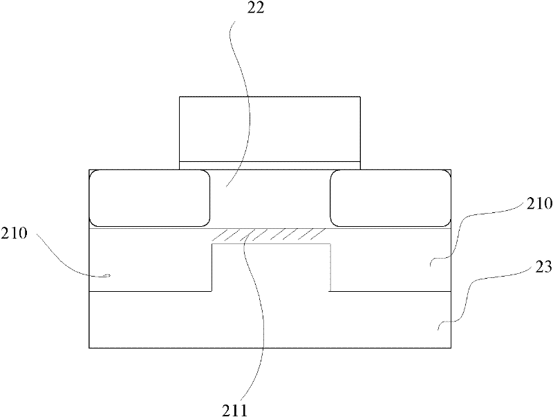
[0021] The first embodiment, FD SOI CMOS.

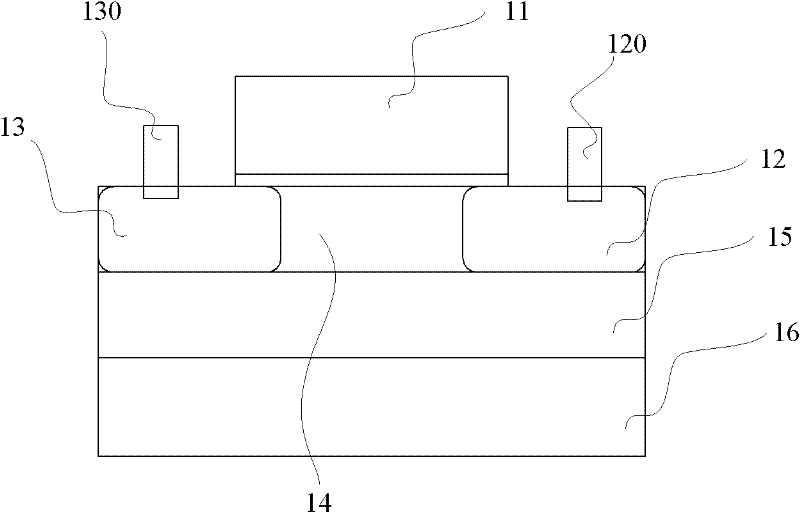
[0022] Reference figure 2 The insulating layer of the FD SOI CMOS is divided into a first insulating layer 211 under the channel region 22 and an uncovered second insulating layer 210. The thickness H1 of the first insulating layer 211 is smaller than the thickness H2 of the second insulating layer 210. Preferably, H1 is 1 / 10 to 1 / 2 of H2. For ordinary thin film FD SOI CMOS, H2 is above 100 nanometers, and for ultra-thin FD SOI CMOS, H2 is between 20 nanometers and 100 nanometers. The SOI substrate composed of the first insulating layer 211, the second insulating layer 210 and the underlying substrate 23 is an embodiment of the SOI substrate provided by the present invention. In the above embodiment, the underlying substrate 23 may be a silicon substrate, and the insulating layer may be silicon dioxide.

[0023] Through device simulation, when the drain voltage is 1V and H1 is the value within the range of the above-mentioned embodimen...

Embodiment 2

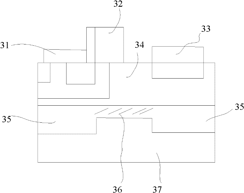
[0027] The second embodiment, SOI LDMOS.

[0028] Reference image 3 , Is a schematic diagram of the structure of an SOI LDMOS device provided by an embodiment of the present invention. The device includes a source 31, a gate 32, a drain 33, a diffusion region 34, an insulating layer, and an underlying substrate 37. The insulating layer includes a third insulating layer 35 and a fourth insulating layer 36. The thickness h3 of the third insulating layer 35 is greater than the thickness h4 of the fourth insulating layer. Compared with existing SOI LDMOS devices, image 3 In the SOI LDMOS device shown, due to the small thickness h4 of the fourth insulating layer, the heat dissipation of the diffusion region 34 is enhanced, and the lattice temperature is significantly reduced. Since the lattice temperature is significantly reduced, the self-heating effect is greatly suppressed, thereby Reduce the degradation of carrier mobility at high temperatures, increase the leakage current of the...


PUM


Abstract

The invention provides a silicon-on-insulator (SOI) substrate structure and an SOI device using the SOI substrate structure, for further reducing the self-heating effect of the SOI device and avoiding the problems of substantially reduced SOI device performance, many process modifications and high cost and the like in the existing scheme of reducing the self-heating effect; meanwhile, by the adoption of the invention, current at a drain terminal can be increased, the off-state leakage current of the device can be reduced and the ratio of on-state current to off-state current can be obviously improved. The SOI substrate structure provided by the invention comprises an insulating layer and a bottom substrate below the insulating layer, wherein the insulating layer is divided into a first insulating layer below a channel region and a second insulating layer beyond the first insulating layer, and the thickness of the first insulating layer or a part of the first insulating layer is smaller than that of the second insulating layer.

Description

Technical field [0001] The present invention relates to the field of semiconductor manufacturing, in particular to a silicon on insulator (SOI, Silicon on Insulator) substrate structure and devices. Background technique [0002] With the advancement of technology, the development of integrated circuits to the ultra-large-scale nanoscale stage. The process of bulk silicon substrates and bulk silicon devices is approaching physical limits, and severe challenges are encountered in further reducing the feature size of integrated circuits. At present, the industry believes that SOI substrates and SOI devices are one of the best solutions to replace bulk silicon substrates and bulk silicon devices. [0003] SOI devices usually have a three-layer structure of "top device / insulating layer / bottom substrate". The full dielectric isolation between the top device and the bottom substrate is achieved through an insulating layer. The insulating layer is usually silicon dioxide, called buried Ox...

Claims


Application Information

Patent Timeline
Patent Type & Authority Applications(China)
IPC IPC(8): H01L27/12H01L21/762
Inventor 苟鸿雁
Owner SHANGHAI HUAHONG GRACE SEMICON MFG CORP
Why Eureka
Try Eureka