Conductive layer under SOI oxygen buried layer and manufacturing process thereof

A manufacturing process and conductive layer technology, applied in the field of microelectronics, can solve the problems that the buried oxide layer cannot be effectively released and restrict the performance of SOI materials, etc., and achieve the effect of reducing the self-heating effect and alleviating the impact

Inactive Publication Date: 2010-12-15
SHANGHAI INST OF MICROSYSTEM & INFORMATION TECH CHINESE ACAD OF SCI +1
View PDF3 Cites 3 Cited by
  • Summary
  • Abstract
  • Description
  • Claims
  • Application Information

AI Technical Summary

Problems solved by technology

However, due to the limitations of the material, it has some defects that are more serious than bulk silicon materials, such as the self-heating effect caused by the inability of the buried oxide layer to effectively release the internal heat and the elevation of the body region due to the charge accumulated at the interface of the buried oxide layer. Potential formation, the so-called floating body effect, etc., all restrict the further performance of SOI materials

Method used


Image

  • Conductive layer under SOI oxygen buried layer and manufacturing process thereof
  • Conductive layer under SOI oxygen buried layer and manufacturing process thereof
  • Conductive layer under SOI oxygen buried layer and manufacturing process thereof

Examples


Embodiment 1

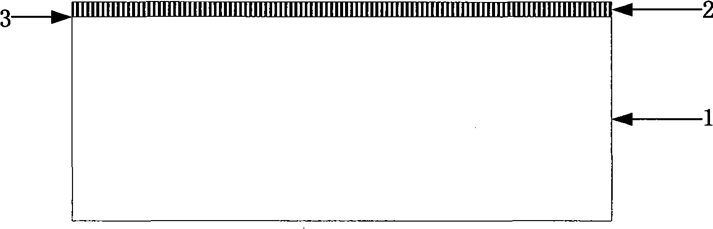
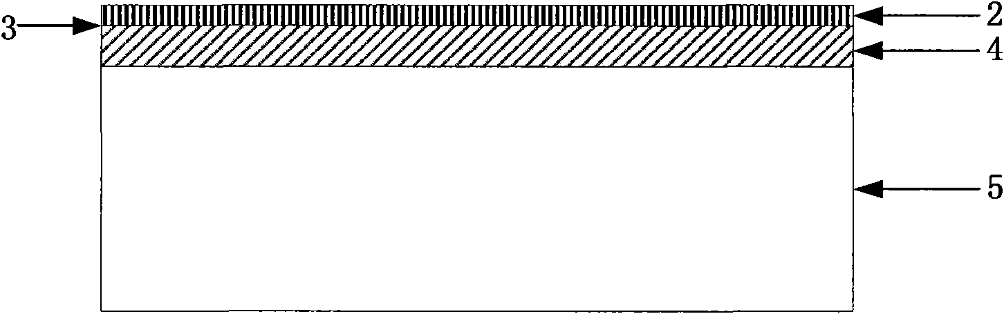
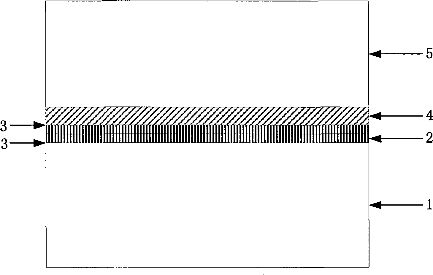
[0038] This embodiment provides a conductive layer under the SOI buried oxide layer, such as Figures 1 to 4 As shown, wherein, the SOI includes a bottom silicon film 1, a buried oxide layer 4, and a top silicon film 5 grown from bottom to top; the conductive layer is grown between the bottom silicon film 1 and the buried oxide layer 4; the conductive The layers comprise a charge guiding layer 2 and a blocking layer 3 grown on the upper and lower surfaces of said charge guiding layer 2 . The charge guiding layer 2 is a conductive metal layer with a melting point higher than 1000°C and difficult to diffuse in an environment of 900°C. The material of the charge guiding layer 2 is copper; the material of the blocking layer 3 is tantalum nitride, and the thickness of the blocking layer 3 is 70, 72, 75, 78 or 80 angstroms.

Embodiment 2

[0040] The difference between this embodiment and the first embodiment is that the charge guiding layer 2 is a non-metallic good conductor layer.

Embodiment 3

[0042] This embodiment provides a manufacturing process of the conductive layer under the SOI buried oxide layer described in Embodiment 1, the process is as follows Figures 1 to 8 shown, including the following steps:

[0043] 1. Deposit a layer of tantalum nitride barrier layer (about 75 angstroms) on the first bulk silicon wafer, and then deposit a layer of metal copper, the thickness of which is 1 / 2 of the thickness of the target metal conductive layer;

[0044] 2. Form a silicon dioxide layer by thermal oxidation on the second bulk silicon wafer, then deposit a layer of tantalum nitride barrier layer (about 75 Angstroms), and finally deposit a layer of metal copper, the thickness of which is the target metal conductive layer 1 / 2 of the thickness;

[0045] 3. Bond the first bulk silicon wafer and the second bulk silicon wafer by metal bonding technology;

[0046] 4. Use hydrogen injection stripping technology to thin the silicon material on the back of the second silico...


PUM

PropertyMeasurementUnit
melting pointaaaaaaaaaa
thicknessaaaaaaaaaa

Abstract

The invention discloses a conductive layer under an SOI oxygen buried layer and a manufacturing process thereof. The SOI comprises a bottom silicon film, an oxygen buried layer and a top silicon film, from bottom to upper, wherein the conductive layer is grown between the bottom silicon film and the oxygen buried layer; the conductive layer comprises a charge conductive layer and a barrier layer; the barrier layer is grown on the upper and lower surfaces of the charge conductive layer. The invention can discharge the heat generated in a device to the exterior through the conductive layer, so as to efficiently decrease the SOI self-heating effect. The effect of non-insulate substrate is as same as the effect of the insulate substrate. Besides, the accumulated surplus charges can be released so as to decrease the influence of the longitudinal electric field on the charge distribution inside the device.

Description

technical field [0001] The invention belongs to the field of microelectronics, and relates to a conductive layer under an SOI buried oxide layer and a manufacturing process thereof. Background technique [0002] With the rapid development of microelectronics technology, the research and development of high-performance, high-integration, and multi-functional ICs have increasingly stringent requirements on materials. Silicon-on-insulator (SOI) materials are new silicon-based integrated circuits. Materials can meet the requirements of the development of microelectronics technology. SOI technology has the characteristics of high circuit speed, high density, radiation resistance, low power consumption, and high temperature resistance. It also has the advantages of simple process flow, high integration, and low soft error rate. It is the key technology to solve the power consumption crisis of VLSI, and is known as "the new silicon-based integrated circuit technology in the 21st ce...

Claims


Application Information

Patent Timeline
Patent Type & Authority Applications(China)
IPC IPC(8): H01L27/12H01L21/762H01L21/3205
Inventor 程新红何大伟王中健徐大伟宋朝瑞俞跃辉
Owner SHANGHAI INST OF MICROSYSTEM & INFORMATION TECH CHINESE ACAD OF SCI
Why Eureka
Try Eureka