Reticle and forming method of semiconductor device

A technology of reticles and semiconductors, which is applied in the direction of equipment, photographic process of patterned surface, and originals used for photomechanical processing, etc. It can solve the problems of overlay accuracy deviation and reduce the ability of imaging system to form accurate patterns, etc., to achieve Improved accuracy, reduced self-heating effect, and high accuracy

Active Publication Date: 2016-06-01
SEMICON MFG INT (SHANGHAI) CORP
View PDF4 Cites 3 Cited by
  • Summary
  • Abstract
  • Description
  • Claims
  • Application Information

AI Technical Summary

Problems solved by technology

[0005] However, some internal reasons of the existing reticle structure, as well as the influence of factors such as the temperature difference o

Method used


Image

  • Reticle and forming method of semiconductor device
  • Reticle and forming method of semiconductor device
  • Reticle and forming method of semiconductor device

Examples


Embodiment Construction

[0043] As mentioned in the background technology, some internal reasons of the existing reticle structure, as well as the influence of factors such as the temperature difference of the reticle at different exposure times, reduce the ability of the imaging system to form accurate patterns, resulting in large overlay accuracy errors .

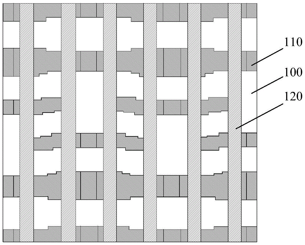
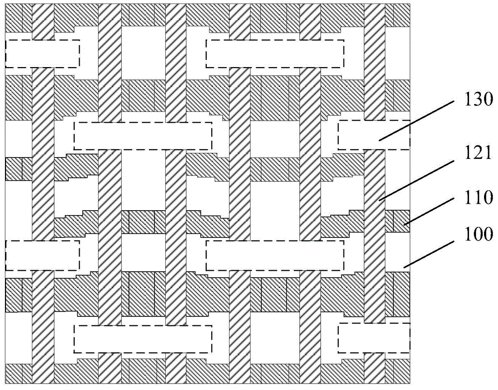
[0044] A reticle generally includes a substrate and a light-shielding layer on the substrate. The shading layer includes a graphic area (the graphic area can also be called a window area or an opening area) and a non-graphic area (the non-graphic area can also be called a non-window area or a non-opening area).

[0045] After analysis, the overlay accuracy error is usually caused by the self-heating effect of the mask. The reason for the self-heating effect of the reticle is as follows: when the reticle is subjected to short-wavelength light such as deep ultraviolet (DUV) light or extreme ultraviolet (EUV) light, the non-patterned area of ​​​​th...


PUM


Abstract

The invention provides a reticle and a forming method of a semiconductor device. The reticle comprises a substrate, a shade layer placed on the substrate and a main pattern placed in the shade layer and further comprises an auxiliary pattern placed in the shade layer, wherein the auxiliary pattern is placed inside the main pattern or at the periphery of the main pattern and is used for increasing the light transmittance of the reticle. The reticle has the advantages that the light transmittance of the reticle is increased due to arrangement of the auxiliary pattern; since the area of the reticle, receiving irradiation of exposure light, is reduced, absorbed light is reduced, the self-heating effect of the reticle is decreased, the self deformation of the reticle is reduced, further the deflection of a device pattern formed by using the reticle can be prevented, and the pattern accuracy of a semiconductor device formed by using the reticle can be improved.

Description

technical field [0001] The invention relates to the field of semiconductor manufacturing, in particular to a mask plate and a method for forming a semiconductor device. Background technique [0002] The manufacture of integrated circuit structures requires the formation of tiny structures with precisely controlled dimensions on silicon substrates, silicon-on-insulator (SOI) substrates, or other suitable semiconductor substrates. A pattern is formed on a semiconductor substrate by performing processes such as lithography, etching, ion implantation, deposition, and oxidation. In order to form tiny structures with precise size control, usually in the pattern generation process stage, a mask layer (mask layer) needs to be formed on the semiconductor substrate, and the mask layer is used to define these tiny structures. [0003] In general, the masking layer may be, for example, a patterned photoresist layer produced by a lithography process, or a hard masking layer that may be ...

Claims


Application Information

Patent Timeline
IPC IPC(8): G03F1/38
Inventor 沈满华祖延雷
Owner SEMICON MFG INT (SHANGHAI) CORP
Why Eureka
Try Eureka