Junction termination structure of transverse high-pressure power semiconductor device

A power semiconductor, lateral high voltage technology, applied in semiconductor devices, electrical components, circuits, etc., can solve problems such as easy concentration of electric field lines, avalanche breakdown, and small radius of curvature

Inactive Publication Date: 2011-11-16
UNIV OF ELECTRONICS SCI & TECH OF CHINA
View PDF6 Cites 56 Cited by
  • Summary
  • Abstract
  • Description
  • Claims
  • Application Information

AI Technical Summary

Problems solved by technology

[0003] The present invention aims at the problems of small curvature radius at the curvature terminal of the lateral high-voltage power semiconductor device with small curvature radius junction terminal, easy concentration of electric field lines, large local electric field at the curvature end, and easy occurre

Method used


Image

  • Junction termination structure of transverse high-pressure power semiconductor device
  • Junction termination structure of transverse high-pressure power semiconductor device
  • Junction termination structure of transverse high-pressure power semiconductor device

Examples


Embodiment Construction

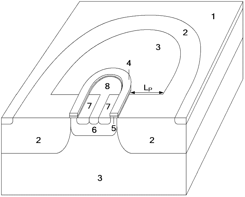
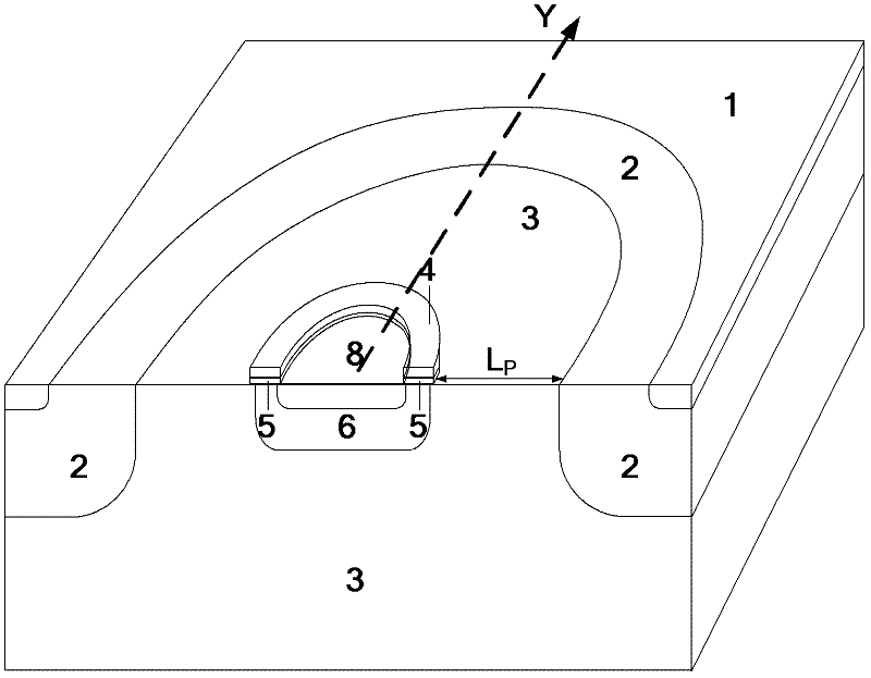
[0030] A junction termination structure for lateral high-voltage power semiconductor devices, such as figure 1 As shown, including straight knot termination structure and curvature junction termination structure.

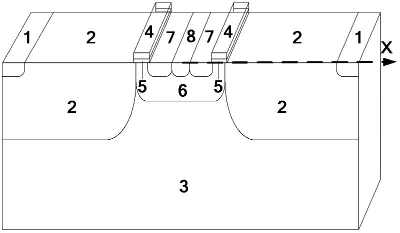
[0031] The linear junction terminal structure is as figure 2 As shown, it has the same structure as the active region of the lateral high-voltage power semiconductor device, including the drain N + Contact region 1, N-type drift region 2, P-type substrate 3, gate polysilicon 4, gate oxide layer 5, P-well region 6, source N + Contact area 7, source P + Contact region 8; P-well region 6 and N-type drift region 2 are located on the upper layer of P-type substrate 3, wherein P-well region 6 is located in the middle, with N-type drift region 2 on both sides, and P-well region 6 and N-type drift region 2 The drift region 2 is connected; the two sides of the N-type drift region 2 away from the P-well region 6 are the drain N + Contact region 1, the upper layer of P-we...


PUM


Abstract

The invention relates to a junction termination structure of a transverse high-pressure power semiconductor device, belonging to the technical field of semiconductor power devices. An N-type drift region at a curvature termination of the transverse high-pressure power semiconductor device is shortened in length to ensure that the N-type drift region is spaced with a P-well region by a certain displace, wherein the spaced part is replaced by a P-type substrate, which is equivalent that additional electric charges of the P-type substrate are introduced so that the peak value of an electric field at a pn junction formed the original P-well region and the N-type drift region is reduced, meanwhile, a new peak value of the electric field is introduced at a pn junction formed by the P-type substrate and the N-type drift region, the radius of curvature of the curvature terminal is increased, the excessive concentration of a power line is avoided, and the puncture voltage of the device is increased, wherein the surface of the N-type drift region also can be combined with a surface RESURF structure or an ultra-junction structure. The junction termination structure has the advantages of being capable of decreasing the width of the curvature terminal of the device, saving the layout area of the device and being compatible with a CMOS (Complementary Metal-Oxide-semiconductor Transistor) process, and can be used for manufacturing the transverse high-pressure power device with the advantages of excellent performance, high voltage, high speed and low conduction loss.

Description

technical field [0001] The invention belongs to the technical field of semiconductor power devices, and relates to a junction terminal structure of a lateral high-voltage power semiconductor device. Background technique [0002] The development of high-voltage power integrated circuits is inseparable from the integration of lateral high-voltage power devices. High-voltage power devices require high breakdown voltage, low on-resistance, and low switching loss. To achieve a high breakdown voltage of a lateral high-voltage power device requires a low doping concentration in the drift region used to bear the withstand voltage, but in order to meet the low on-resistance of the device, it also requires a high doping concentration in the drift region as a current channel . The contradictory relationship between the specific on-resistance of MOS devices and the withstand voltage of the devices limits the application of such devices in the field of high voltage and high current. L...

Claims


Application Information

Patent Timeline
IPC IPC(8): H01L29/06H01L29/78
CPCH01L29/7835H01L29/0634H01L29/0692H01L29/4238
Inventor 乔明温恒娟胡曦王猛庄翔周锌何逸涛
Owner UNIV OF ELECTRONICS SCI & TECH OF CHINA
Why Eureka
Try Eureka