ESD (Electro Spark Detector) power clamping circuit

A technology of clamping circuit and power supply, which is applied in the direction of circuit devices, emergency protection circuit devices, emergency protection circuit devices for limiting overcurrent/overvoltage, etc., to avoid false triggering and reduce the layout area.

Active Publication Date: 2011-11-23
PEKING UNIV
View PDF5 Cites 10 Cited by
  • Summary
  • Abstract
  • Description
  • Claims
  • Application Information

AI Technical Summary

Problems solved by technology

This poses new challenges to the design of ESD power supply clamping circuits

Method used


Image

  • ESD (Electro Spark Detector) power clamping circuit
  • ESD (Electro Spark Detector) power clamping circuit
  • ESD (Electro Spark Detector) power clamping circuit

Examples


Embodiment 1

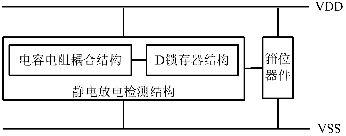
[0040] Such as Figure 4 As shown, the clamping device in this embodiment is an NMOS transistor 60 .

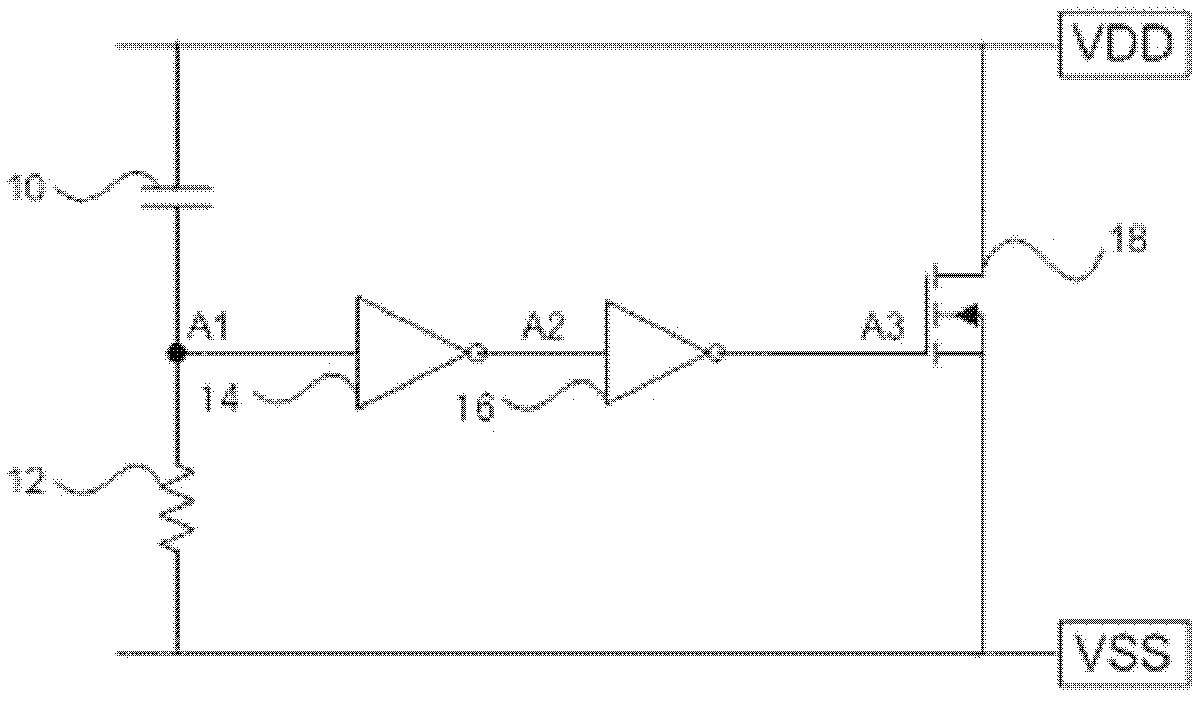
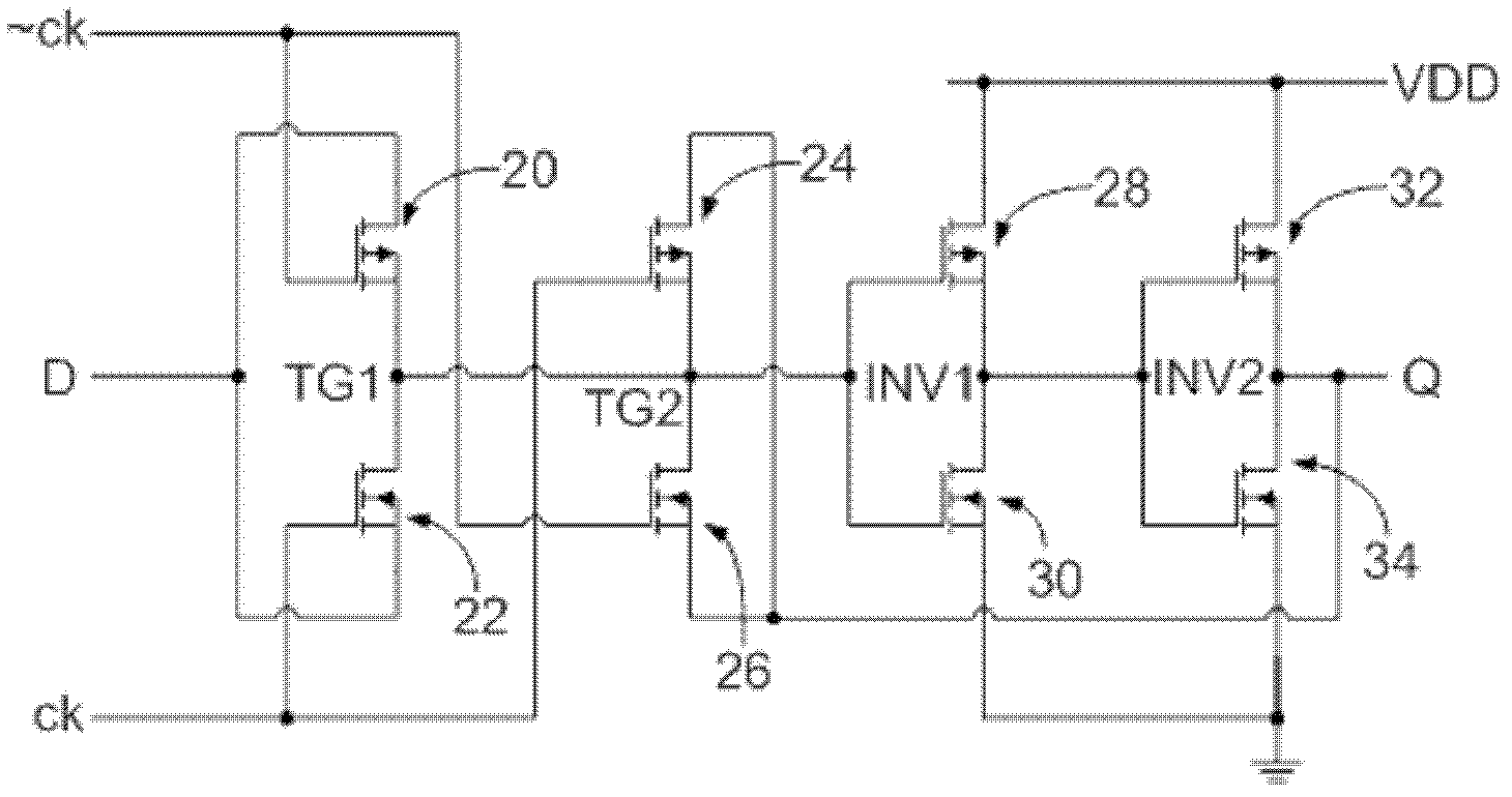
[0041] The D latch structure includes: a first inverter 44, a first CMOS transmission gate TG3, a second CMOS transmission gate TG4, a second inverter 54, a third inverter 56, and a third NMOS transistor 58; The input terminal of an inverter 44 is connected to the connection point C1 of the capacitor 40 and the resistor 42 (the connection point C1 outputs a detection voltage, which is used as the clock signal of the D latch structure, that is figure 2 ck signal in); the two gates of the first CMOS transmission gate TG3 are respectively connected to the input terminal and the output terminal of the first inverter 44 (the complementary signal of the output node C2 output clock signal, namely figure 2 ~ck signal in ), the input control signals are the voltages of nodes C1 and C2 respectively, the input of the first CMOS transmission gate TG3 is connected to the power supply p...

Embodiment 2

[0052]The ESD power supply clamping circuit of this embodiment is a simplification of the circuit of Embodiment 1. Since the input of the D latch structure is connected to a constant high level, the first CMOS transmission gate TG3 can be simplified into an NMOS transmission gate; at the same time, the NMOS transistors in the first inverter 44 and the second CMOS transmission gate TG4 are removed, Only the PMOS transistors in the second CMOS transmission gate TG4 remain. This simplification process does not affect the realization of circuit functions. The HSPICE simulation proves that the function of the circuit after simplification is basically the same as that before simplification.

[0053] Such as Figure 5 As shown, the clamping device of this embodiment is an NMOS transistor 84, and the D latch structure includes: a first NMOS transistor 74, a first PMOS transistor 76, a second NMOS transistor 82, a first inverter 78, and a second inverter Phase device 80; the gate of...


PUM


Abstract

The invention discloses an ESD (Electro Spark Detector) power clamping circuit and relates to the technical field of ESD protection of a semiconductor integrated chip. The ESD power clamping circuit comprises a power pin VDD, a grounded pin VSS, a static discharging detection structure and a clamping component, wherein the static discharging detection structure and the clamping component are connected between the power pin VDD and the grounded pin VSS; the static discharging detection structure further comprises a capacitance-resistance coupling structure and a D latch structure; the capacitance-resistance coupling structure is composed of a capacitor and a resistor serially connected between the power pin VDD and the grounded pin VSS and is used for detecting and outputting a static discharging voltage on the power pin VDD or the grounded pin VSS; and the D latch structure is connected between a joint of the capacitor and the resistor and a grid electrode of a clamping transistor andis used for sending a voltage outputted by the capacitance-resistance coupling structure to the clamping component. The ESD power clamping circuit provided by the invention has a small layout area and can be used for efficiently preventing a spurious triggering phenomenon.

Description

technical field [0001] The invention relates to the technical field of electrostatic discharge (ESD) protection of semiconductor integrated chips, in particular to an ESD power supply clamping circuit based on a D latch. Background technique [0002] ESD issues have long been a major threat to the reliability of the semiconductor industry. It is reported that more than 70% of damages to integrated circuits (Integrated Circuits, IC) are caused by ESD or electrical overstress (Electrical Overstress, EOS). With the scaling down of Complementary Metal Oxide Semiconductor (CMOS) technology, the gate oxide layer of devices is getting thinner and the junction depth is getting shallower, making CMOS circuits more susceptible to ESD damage. Therefore, an effective ESD protection circuit must be added between each input / output interface (I / O pin) to provide a low-impedance discharge path for electrostatic charges. In addition, since the core circuit is directly connected between the...

Claims


Application Information

Patent Timeline
Patent Type & Authority Applications(China)
IPC IPC(8): H02H9/04
Inventor 张雪琳王源贾嵩张钢刚张兴
Owner PEKING UNIV
Why Eureka
Try Eureka