Supercharge Your Innovation With Domain-Expert AI Agents!

Optical semiconductor device lead frame and manufacturing method thereof

A technology for optical semiconductor devices and manufacturing methods, which is applied to semiconductor devices, electrical solid-state devices, electrical components, etc., can solve problems such as reflectivity decline, brightness decline, and roughness influence, and achieves excellent long-term stability of reflectivity and reflection. The effect of good characteristics and excellent reflection characteristics

Inactive Publication Date: 2014-07-23
FURUKAWA ELECTRIC CO LTD
View PDF7 Cites 2 Cited by
  • Summary
  • Abstract
  • Description
  • Claims
  • Application Information

AI Technical Summary

Problems solved by technology

[0005] However, in the case of simply forming a film of silver or its alloy as in the technology disclosed in Patent Document 1, it is unavoidable that the wavelength in the ultraviolet region is greatly reduced, and the reflectance in the visible region from around 400nm to around 300nm is unavoidable.
[0006] In addition, if the crystal grain size is formed to be 0.5 μm or more as in the technology disclosed in Patent Document 2, the reflectance in the visible light region is definitely slightly improved, but the wavelength of 400 nm or less appears to be the same as that disclosed in Patent Document 1. The same phenomenon as the technology, the decrease in reflectance in the ultraviolet region cannot be avoided
In addition, if the crystal grain size is adjusted to the above-mentioned by heat treatment, it is presumed that silver is oxidized due to the influence of residual oxygen, and the reflectance decreases instead, so that a sufficient effect of improving the reflectance cannot be obtained.
[0007] Furthermore, Patent Document 2 discloses that the maximum height Ry of the base material of the surface layer silver film is set to be 0.5 μm or more in surface roughness, but the factor that constitutes the reflection phenomenon of light is not the roughness of the base portion, but the surface layer near the outermost layer. The thickness of the
Therefore, a silver film is formed on the substrate or substrate plating by electroplating or vapor deposition to form a reflective layer, so it may be meaningless even to define the roughness of the substrate.
In addition, Ry refers to the difference between the maximum value and the minimum value of the roughness, and it is likely to indicate only the unevenness of a specific part of the surface, such as the numerical value of a small part such as a scratch formed in a line, and does not indicate the overall value that depends on reflection. The thickness of the range, so Ry is sometimes not suitable as a parameter to represent the characteristics of the reflective layer
[0008] Furthermore, when the lead frame produced by the technique disclosed in the above document is used for an LED, the luminance decreases over time.
As a result of the investigation, it was found that the silver on the surface of the lead frame is sulfurized due to the small amount of sulfur contained in the sealing resin, so the silver turns black and the brightness decreases.
In addition, sterling silver is prone to migration
[0009] In addition, in the lead frame disclosed in Patent Document 3, compared with silver, rhodium reduces the reflection characteristics important for optical semiconductor devices, especially the reflectance including the visible light region, such as the wavelength 400 to 800 nm, by 20%. As mentioned above, if only thin rhodium is simply coated, blue or white optical semiconductor devices cannot meet the required characteristics of reflectance.

Method used


Image

  • Optical semiconductor device lead frame and manufacturing method thereof
  • Optical semiconductor device lead frame and manufacturing method thereof
  • Optical semiconductor device lead frame and manufacturing method thereof

Examples


Embodiment 1

[0072] The substrates shown in Table 1 with a thickness of 0.3 mm and a width of 50 mm were subjected to the following pretreatment, and then subjected to the following electroplating treatment to obtain Inventive Examples 1 to 39, Conventional Example 1, and Comparative Example 1 having the configurations shown in Table 1. , 2 lead frames.

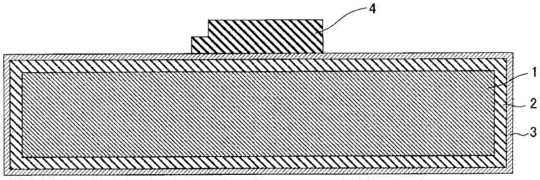
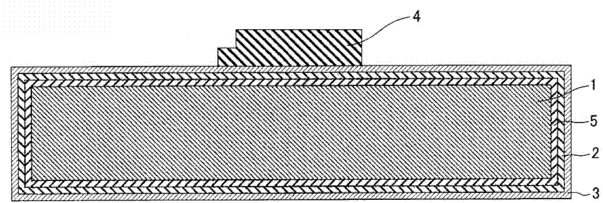
[0073] The layer structure of each lead frame is formed according to the order of substrate, pure silver layer and outermost film in Examples 1 to 6 of the present invention, and is formed according to the order of substrate, base layer and pure silver layer in prior example 1, the present invention In Examples 7 to 39 and Comparative Examples 1 and 2, the matrix, base layer, pure silver layer, and outermost film were formed in this order. In addition, the pure silver layer was formed to a thickness of 1 μm in all examples under the following Ag plating conditions, and before the outermost layer film was formed, it was measured by a conta...

Embodiment 2

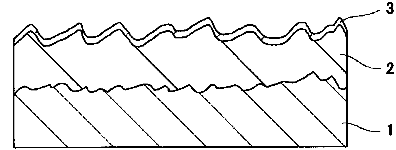
[0158] On a copper alloy made of C19400 with a thickness of 0.15 mm and a width of 30 mm, a nickel plating layer was formed as a base layer with a thickness of 1.0 μm, a pure silver layer was formed on top of it, and the thickness shown in Table 3 was formed as the outermost layer The Pt electroplated layer of the present invention obtained the lead frames of Examples 40-63 and Comparative Examples 3-7. Each plating step or the composition of the plating solution was the same as in Example 1, and glossy silver plating and matte silver plating were used for the formation of the pure silver layer. In addition, when adjusting the Ra and plating thickness of the pure silver layer, in glossy silver plating and matte silver plating, use 0.1-10A / dm 2 Conditions to adjust the current density. In addition, Ra of the pure silver layer was measured with a contact-type surface roughness meter (SURFCORDER SE-30H (trade name): manufactured by Kosaka Laboratories) in the same manner as in E...


PUM

PropertyMeasurementUnit
heightaaaaaaaaaa
thicknessaaaaaaaaaa
thicknessaaaaaaaaaa

Abstract

The present invention provides a lead frame for an optical semiconductor device and a manufacturing method thereof. In this lead frame, a pure silver layer made of pure silver is formed on the substrate. The arithmetic mean height Ra of the pure silver layer is 0.001-0.2 μm, and an average film made of a metal material with excellent corrosion resistance is formed on the surface. A film with a thickness of not less than 0.001 μm and not more than 0.2 μm. The lead frame for an optical semiconductor device has excellent reflection properties in the visible light region and excellent corrosion resistance.

Description

technical field [0001] The present invention relates to a lead frame for an optical semiconductor device and a manufacturing method thereof. Background technique [0002] Lead frames for optical semiconductor devices are currently widely used as various display and illumination light sources using LED elements and the like as light sources. In this optical semiconductor device, for example, a lead frame is arranged on a substrate, and after a light-emitting element is mounted on the lead frame, the light source is encapsulated with a sealing resin to prevent deterioration of the light source or its surrounding parts caused by heat, moisture, oxidation, etc. and its surroundings are sealed. [0003] In addition, directly below the light source, a layer of silver or a silver alloy having excellent light reflection characteristics is often formed. There is a content that the reflection characteristics are improved by setting the crystal grain size of the silver or silver allo...

Claims


Application Information

Patent Timeline
Patent Type & Authority Patents(China)
IPC IPC(8): H01L33/62
CPCH01L33/62H01L2924/0002H01L2924/00
Inventor 小林良聪小关和宏菊池伸
Owner FURUKAWA ELECTRIC CO LTD
Features
  • R&D
  • Intellectual Property
  • Life Sciences
  • Materials
  • Tech Scout
  • Unparalleled Data Quality
  • Higher Quality Content
  • 60% Fewer Hallucinations
Learn More