One-hole welding mold and welding process for electronic components

A technology of electronic components and welding process, which is applied in the field of electronic component one-hole welding mold and welding process, which can solve the problems of gaps and large apertures of welding molds, etc., and achieve the effects of increasing yield, high welding precision, and cost saving

A technology of electronic components and welding process, which is applied in the field of electronic component one-hole welding mold and welding process, which can solve the problems of gaps and large apertures of welding molds, etc., and achieve the effects of increasing yield, high welding precision, and cost saving

CN102259247AInactive Publication Date: 2011-11-30许行彪

Image

  • One-hole welding mold and welding process for electronic components
  • One-hole welding mold and welding process for electronic components
  • One-hole welding mold and welding process for electronic components

Examples


Embodiment Construction

[0027] The present invention will be further described below in conjunction with the accompanying drawings and embodiments.

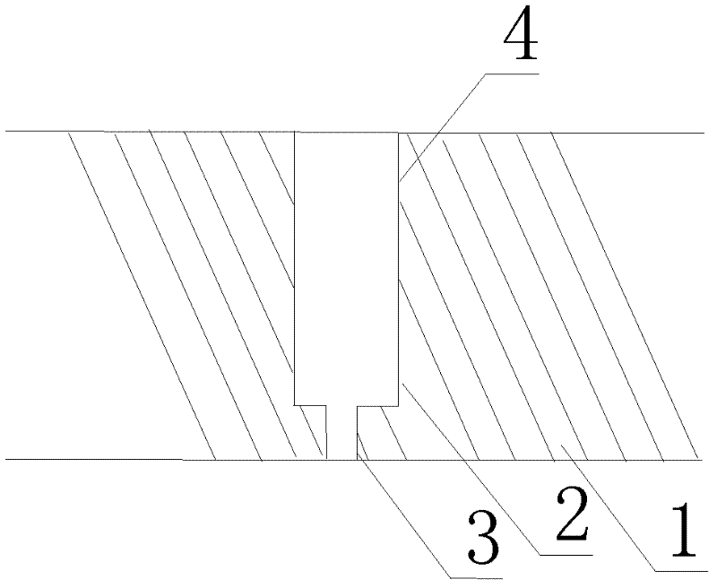
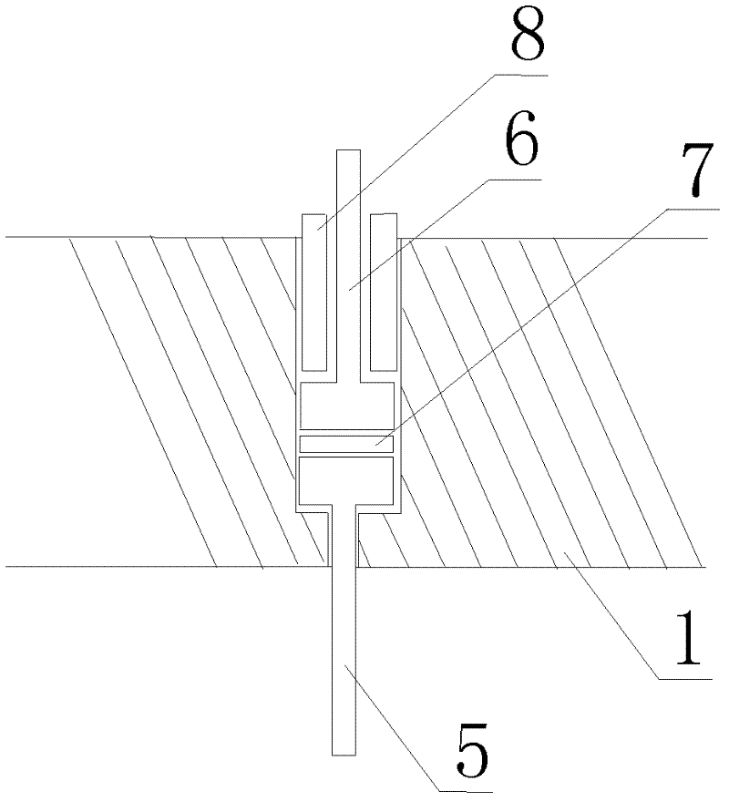
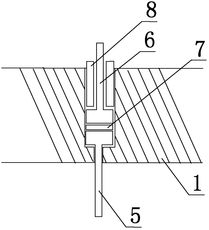
[0028] Such as figure 1 Shown, a kind of electronic component one-hole welding mold, it comprises welding mold body 1, is provided with a plurality of positioning welding molds 2 for placing electronic components on welding mold body 1, and the material of described welding mold body 1 is nitrogen Silicon or graphite, the positioning welding mold 2 is composed of a small hole 3 and a counterbore 4, the small hole 3 and the counterbore 4 run through, and the center coincides; the small hole 3 is used to place the lead end of the lower lead 5, and the aperture of the small hole 3 is the same as The lead end of the lower lead 5 matches; the counterbore 4 is used to place the head of the lower lead 5 , the chip 7 and the upper lead 6 , and the aperture of the counterbore 4 matches the head of the lower lead 5 .

[0029] The welding mold body 1 of the prese...


PUM


Abstract

A one-hole welding mold for electronic components and a welding process, comprising a welding mold body (1), a plurality of positioning welding molds (2) for placing electronic components on the welding mold body (1), the positioning welding The die (2) consists of a small hole (3) and a countersunk hole (4), the small hole (3) and the countersunk hole (4) pass through, and the centers coincide; the small hole (3) is used to place the lead end of the lower lead (5). , the aperture of the small hole (3) is matched with the lead end of the lower lead (5); the countersunk hole (4) is used to place the head of the lower lead (5), the chip (7) and the upper lead (6), The hole diameter of (4) is matched with the head of the lower lead (5). In the present invention, the upper and lower leads and the semiconductor chip are welded in the same hole, and the welding precision is high, and there is no need to worry about welding dislocation and virtual welding, and the product quality and yield are greatly improved.

Description

technical field [0001] The invention relates to a welding mold for electronic components and a welding process using the mold, in particular to a welding forming process using a single mold, in particular to a one-hole welding mold for electronic components and a welding process. Background technique [0002] Now, the traditional welding process of electronic components (diode, etc.) is the process of welding the upper and lower welding dies. The traditional welding consists of a lead wire on the upper welding die and a lower welding die on each of the upper and lower soldering dies. The aperture is generally about 0.1-0.15mm larger than the diameter of the lead wire. In addition, the upper and lower dies need to be positioned and matched. There is a fit gap during welding, which is prone to welding misalignment and the weld is not tight; at the same time, due to the oxidation of the welding die at high temperature, the aperture As the size increases, it will cause more seri...

Claims


Application Information

Patent Timeline
30 Nov 2011
Publication
CN102259247A
IPC
B23K37/04; H01L21/60
CPC
H01L24/01
Inventors
许行彪