Check patentability & draft patents in minutes with Patsnap Eureka AI!

Method of forming a discrete gate memory device

A storage device and discrete gate technology, which is applied in the direction of semiconductor devices, semiconductor/solid-state device manufacturing, electrical components, etc., can solve the problems that the process accuracy cannot meet the corresponding requirements, and achieve the effects of easy control of process accuracy, low cost, and simple process

Inactive Publication Date: 2011-11-30
SEMICON MFG INT (SHANGHAI) CORP +1
View PDF5 Cites 5 Cited by
  • Summary
  • Abstract
  • Description
  • Claims
  • Application Information

AI Technical Summary

Problems solved by technology

[0012] The above-mentioned method of forming a floating gate with a sharp edge adopts the process of partial thermal oxidation and then wet etching. Due to the limitation of the precision of the local thermal oxidation and wet etching process, it is only applicable to flash memory with larger feature size. For feature size For the flash memory structure below 130nm, the process precision cannot meet the corresponding requirements

Method used


Image

  • Method of forming a discrete gate memory device
  • Method of forming a discrete gate memory device
  • Method of forming a discrete gate memory device

Examples


Embodiment Construction

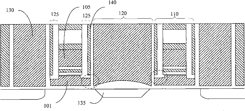
[0029] Theoretically speaking, the tunnel thermal electron emission mechanism is used in the programming of discrete gate memory devices to make the programming rate faster, and the response time is generally on the order of μs; while the F-N tunneling effect is used to make the erasing rate slower when erasing information. , in the order of ms. According to the F-N tunneling effect current formula,

[0030] i FN =A×S TUN ×E 2 TUN ×exp(B / E TUN )

[0031] Among them, E TUN is the electric field strength in the tunneling insulating layer, S TUN is the area of ​​electron tunneling between the floating gate and the erasing gate, and A and B are F-N parameters. The tunneling current i FN and the field strength E on the tunneling insulating layer TUNClosely related, in order to increase the electric field strength, the thickness of the tunneling insulating layer can be reduced, but this will easily cause the loss of charge on the floating gate, resulting in the loss of inf...


PUM


Abstract

The present invention provides a method for forming a discrete gate storage device, comprising: providing a semiconductor substrate, and sequentially forming a gate dielectric layer, a first polysilicon layer, an interlayer insulating layer and a second polysilicon layer on the semiconductor substrate layer; etch the second polysilicon layer and the interlayer insulating layer until the first polysilicon layer is exposed to form a control gate; form sidewalls on the sidewalls of the control gate and the etched interlayer insulating layer ; Using the control gate and the sidewall as a mask, using an isotropic plasma etching process to etch the first polysilicon layer, so that the outside of the etched first polysilicon layer has a sharp point. Compared with the prior art, the process of the invention is simple and low in cost, and because the precision of the plasma etching process is easy to control, it is more suitable for the manufacture of devices with small feature sizes.

Description

technical field [0001] The invention relates to a semiconductor manufacturing process, in particular to a method for forming a discrete gate storage device. Background technique [0002] In the current semiconductor industry, integrated circuits can be divided into three main types: analog integrated circuits, digital integrated circuits and digital / analog hybrid integrated circuits. [0003] As an important type of digital integrated circuits, storage devices, especially flash memory (flash memory, referred to as flash memory) are developing rapidly, mainly because flash memory can store information for a long time without power on, and has a high degree of integration. , fast access speed, easy to erase and rewrite, etc. [0004] The standard physical structure of flash memory is called a memory cell (bit). The structure of the memory cell is different from that of conventional MOS transistors. The gate (gate) of a conventional MOS transistor and the conductive channel ...

Claims


Application Information

Patent Timeline
IPC IPC(8): H01L21/8247H01L21/28
Inventor 李凤莲洪中山何其旸
Owner SEMICON MFG INT (SHANGHAI) CORP
Features
  • R&D
  • Intellectual Property
  • Life Sciences
  • Materials
  • Tech Scout
  • Unparalleled Data Quality
  • Higher Quality Content
  • 60% Fewer Hallucinations
Learn More