
Power MOS (metal oxide semiconductor) component for transversely diffusing metallic oxides

A technology of MOS devices and oxides, which is applied in semiconductor devices, electrical components, circuits, etc., can solve the problems of mutual depletion, lower breakdown voltage, and large on-resistance, so as to improve high-voltage resistance and reduce specific conduction Resistance, the effect of reducing the electric field strength

Inactive Publication Date: 2013-04-03
SUZHOU VOCATIONAL UNIV
View PDF5 Cites 0 Cited by
  • Summary
  • Abstract
  • Description
  • Claims
  • Application Information

AI Technical Summary

Problems solved by technology

[0003] Although the Single RESURF structure can meet a certain breakdown voltage requirement, the on-resistance is relatively large due to the low concentration of the drift region
If the implant dose in the drift region is too large to cause partial depletion, the electric field in the junction between the P-type well layer and the N-type lightly doped layer close to the channel region reaches the critical electric field of the silicon material in advance and breakdown occurs, The breakdown voltage is reduced; if the implantation dose of the drift region is too low to completely deplete and at the same time part of the drain region is also depleted, the junction between the drain region near the drain end and the N-type lightly doped layer is premature Breakdown occurs, which also reduces the breakdown voltage
It is reported in the prior art that a P-type lightly doped region is implanted on the surface of the N-type lightly doped layer, thereby improving the surface electric field distribution in the drift region. Although this design can increase the breakdown voltage, it is not conducive to reducing the specific on-resistance design of the device. ; and will lead to inhomogeneous electric field and mutual depletion, which will lead to lower cut-off frequency of LDMOS devices

Method used


Image

  • Power MOS (metal oxide semiconductor) component for transversely diffusing metallic oxides
  • Power MOS (metal oxide semiconductor) component for transversely diffusing metallic oxides
  • Power MOS (metal oxide semiconductor) component for transversely diffusing metallic oxides

Examples


Embodiment

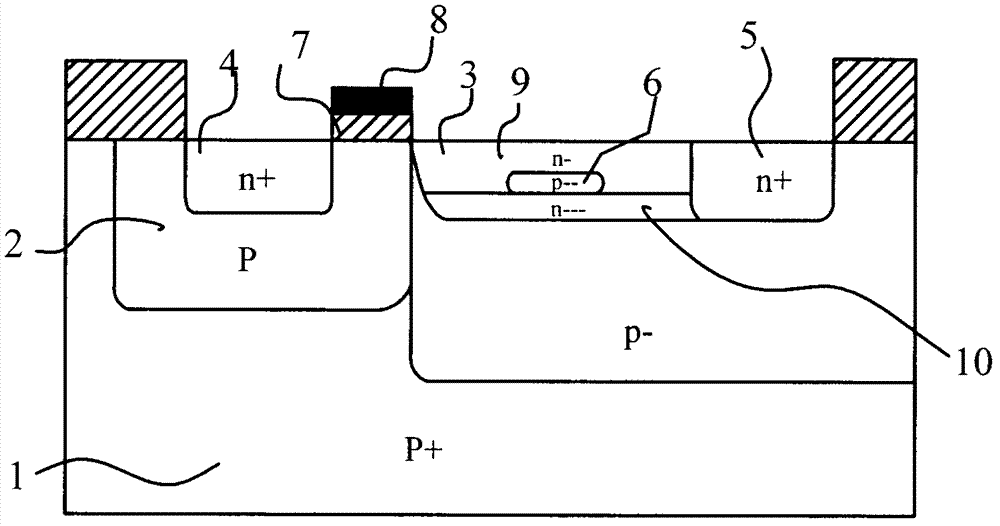
[0023] Embodiment: A laterally diffused metal oxide power MOS device, comprising: a P-type well layer 2 and an N-type lightly doped layer 3 located in a P-type substrate layer 1, and the P-type well layer 2 and the N-type lightly doped layer The doped layers 3 are adjacent in the horizontal direction to form a PN junction, a source region 4 is located in the P-type well layer 2, a drain region 5 is located in the substrate layer 1, and a drain region 5 is located in the source region 4 and A gate oxide layer 7 is provided above the P-type well layer 2 in the area between the N-type lightly doped layers 3, and a gate region 8 is provided above the gate oxide layer 7; the N-type lightly doped layer 3 is composed of the first N Type lightly doped region 9, second N-type lightly doped region 10 and P-type lightly doped region 6; the doping concentration of the first N-type lightly doped region 9 is higher than that of the P-type lightly doped region The doping concentration of the...


PUM


Abstract

The invention discloses a power MOS (metal oxide semiconductor) component for transversely diffusing metallic oxides, comprising a P-type trap layer and an N-type light dope layer, which are arranged in a P-type substrate layer, wherein the N-type light dope layer comprises a first N-type light doping area, a second N-type light doping area and a P-type light doping area; the doping density of the first N-type light doping area is higher than that of the P-type light doping area; the doping density of the P-type light doping area is higher than that of the second N-type light doping density; the first N-type light doping area is arranged above the second N-type light doping area; and the P-type light doping area is arranged in the central area of the first N-type light doping area in the horizontal direction, and the P-type light doping area is arranged at the low medium part in the central area of the first N-type light doping area in the vertical direction and contacted with the surface of the second N-type light doping area. The power MOS component improves the breakdown voltage and reduces the specific on-resistance of a device, and improves the response time and the frequencycharacteristic of the device greatly.

Description

technical field [0001] The invention relates to a MOS device, in particular to a lateral diffusion metal oxide power MOS device. Background technique [0002] Laterally diffused metal oxide power MOS devices (LDMOS); with the rapid development of the semiconductor industry, power electronics technology represented by high-power semiconductor devices has developed rapidly, and its application fields have continued to expand, such as the control of AC motors and printer drive circuits. Among all kinds of power devices today, LDMOS has high working voltage and relatively simple process, so LDMOS has broad development prospects. In the design of LDMOS devices, the breakdown voltage and on-resistance have always been the main goals that people pay attention to when designing such devices. The thickness of the epitaxial layer, doping concentration, and the length of the drift region are the most important parameters of LDMOS. The breakdown voltage can be increased by increasing t...

Claims


Application Information

Patent Timeline
Patent Type & Authority Patents(China)
IPC IPC(8): H01L29/06H01L29/36H01L29/78
CPCH01L29/7835H01L29/0634
Inventor 陈伟元
Owner SUZHOU VOCATIONAL UNIV
Learn More