
Semiconductor device

a technology of a semiconductor and a gate electrode, which is applied in the direction of semiconductor devices, basic electric elements, electrical equipment, etc., can solve the problems that the high electric field generated at the gate electrode end cannot be effectively relaxed, and achieve the effects of reducing cgd, increasing gain, and reducing current collaps

Active Publication Date: 2017-05-30
PANASONIC INTELLECTUAL PROPERTY MANAGEMENT CO LTD
View PDF30 Cites 3 Cited by
  • Summary
  • Abstract
  • Description
  • Claims
  • Application Information

AI Technical Summary

Benefits of technology

[0014]Thus, it is an object of the present invention to achieve both of an increase in gain by increasing a thickness of a gate electrode to reduce Rg, and an increase in gain by forming a source field plate to relax an electric field, and reduce Cgd.
[0016]According to the present invention, useful effects concerning an increase in gain can be obtained by reducing a current collapse, reducing Cgd, and reducing Rg.

Problems solved by technology

Meanwhile, according to the patent literature 2, in the case where the source field plate is formed on a side of the gate electrode part, a certain gap is generated between the gate electrode and the field plate electrode, so that the high electric field generated at the gate electrode end cannot be effectively relaxed.

Method used


Image

  • Semiconductor device
  • Semiconductor device
  • Semiconductor device

Examples


first exemplary embodiment

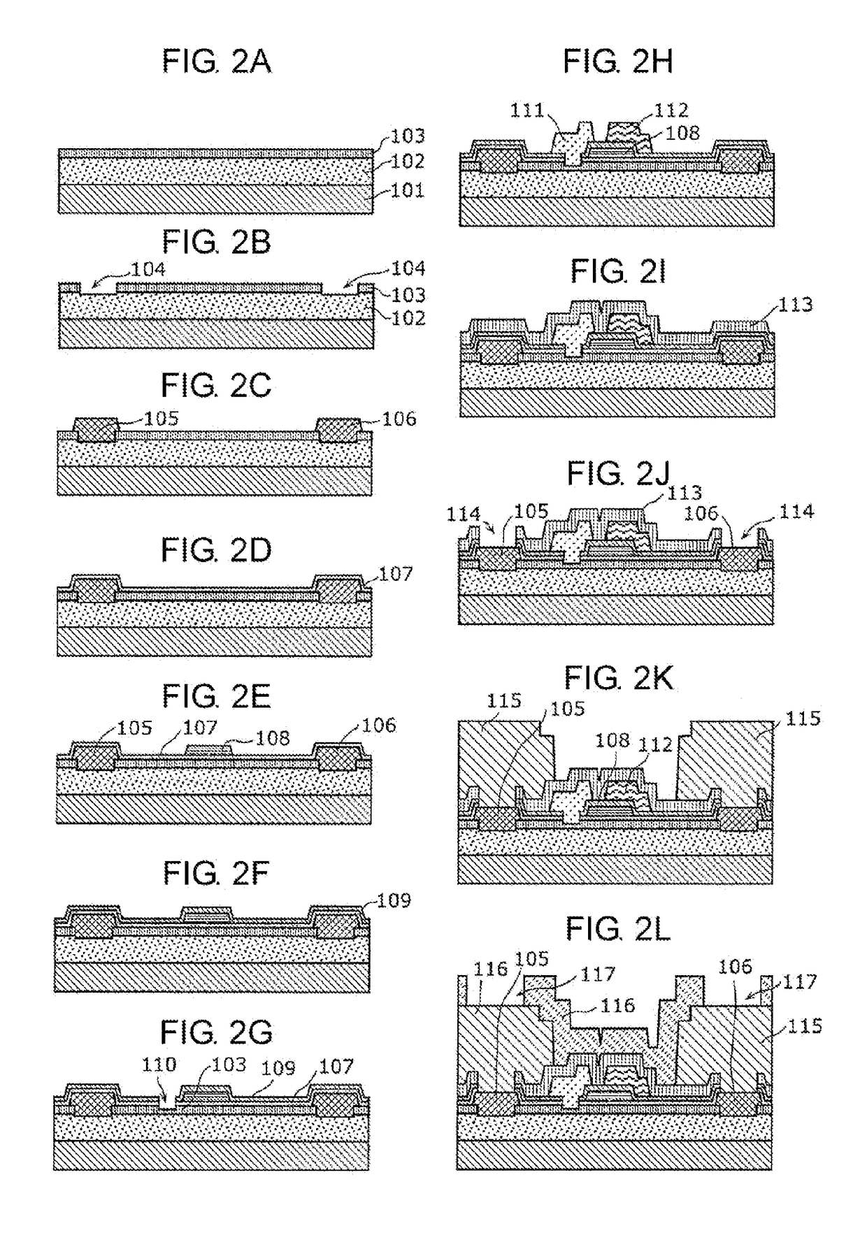
[0076]Hereinafter, a description will be given to a structure and a manufacturing method of a semiconductor device according to the first exemplary embodiment of the present invention.

[0077](Description of Structure)

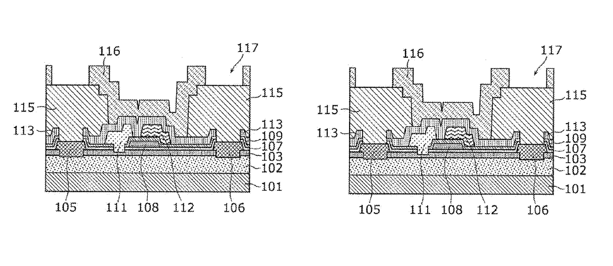
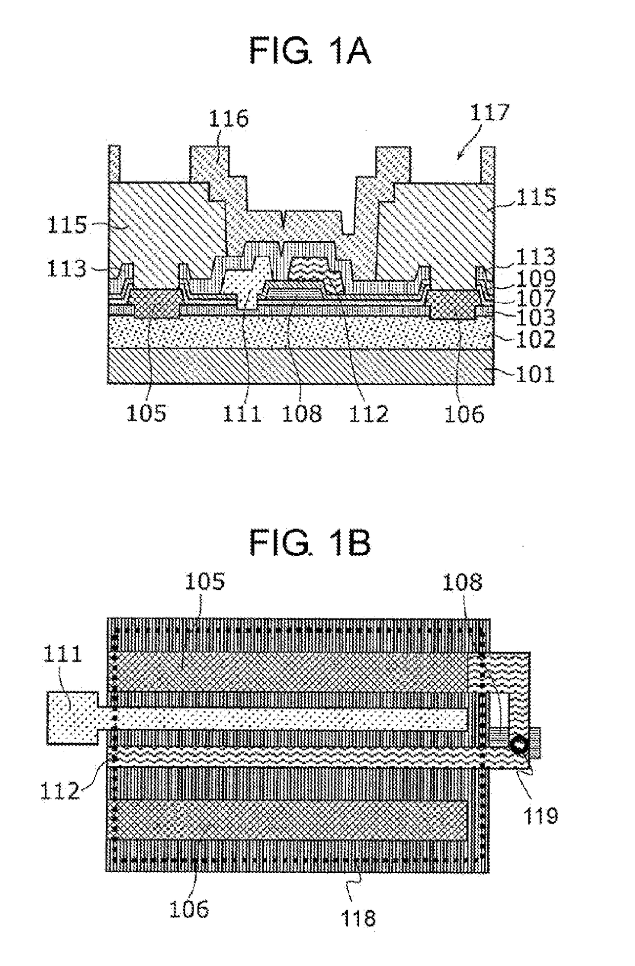
[0078]FIGS. 1A and 1B are a cross-sectional view and a top view of the semiconductor device according to the first exemplary embodiment, respectively.

[0079]As illustrated in FIG. 1A, first semiconductor layer 102 made of a Group III nitride semiconductor, and second semiconductor layer 103 made of a Group III nitride semiconductor are disposed on substrate 101 made of silicon (Si), gallium nitride (GaN), sapphire, or SiC, for example. In addition, first semiconductor layer 102 is favorably made of GaN, for example and second semiconductor layer 103 is favorably made of AlGaN such as AlxGa1-xN, for example (x=0.3, for example). Here, it is favorable that a bandgap in second semiconductor layer 102 is larger than a bandgap in a channel region of first semiconductor layer 1...

second exemplary embodiment

[0110]Hereinafter, a description will be given to a structure and a manufacturing method of a semiconductor device according to the second exemplary embodiment of the present invention.

[0111](Description of Structure)

[0112]FIGS. 3A and 3B are a cross-sectional view and a top view of the semiconductor device according to the second exemplary embodiment, respectively.

[0113]As for a main different point between this exemplary embodiment illustrated in FIG. 3A and the first exemplary embodiment illustrated in FIG. 1A, according to this exemplary embodiment, first field plate electrode 208 is directly connected to second field plate electrode 213 through an opening formed in second protective film 209.

[0114]In addition, configurations of substrate 201, first semiconductor layer 202, second semiconductor layer 203, source electrode 205, drain electrode 206, first protective film 207, first field plate electrode 208, second protective film 209, gate electrode 212, second field plate electr...

third exemplary embodiment

[0124]Hereinafter, a description will be given to a structure and a manufacturing method of a semiconductor device according to the third exemplary embodiment of the present invention.

[0125](Description of Structure)

[0126]FIGS. 5A and 5B are a cross-sectional view and a top view of the semiconductor device according to the third exemplary embodiment, respectively.

[0127]As for a main different point between this exemplary embodiment illustrated in FIG. 5A and the first exemplary embodiment illustrated in FIG. 1A, according to this exemplary embodiment, first field plate electrode 308 is directly connected to second field plate electrode 309. Especially, according to this exemplary embodiment, a whole lower surface of second field plate electrode 309 is directly connected to an upper surface of first field plate electrode 308.

[0128]In addition, configurations of substrate 301, first semiconductor layer 302, second semiconductor layer 303, source electrode 305, drain electrode 306, fir...


PUM


Abstract

An object is to achieve an increase in gain by reducing a current collapse, and reducing Cgd and Rg. A semiconductor device according to the present invention includes a substrate; a first semiconductor layer disposed on the substrate and made of a Group III nitride semiconductor; a second semiconductor layer disposed on the first semiconductor layer and made of a Group III nitride semiconductor; a gate electrode, a source electrode, and a drain electrode disposed on the second semiconductor layer; a first field plate electrode disposed on the second semiconductor layer; and a second field plate electrode disposed on the first field plate electrode, in which the first field plate electrode and the second field plate electrode are disposed between the gate electrode and the drain electrode.

Description

TECHNICAL FIELD[0001]The present invention relates to a semiconductor device and a method for manufacturing the same, and more particularly to a semiconductor device concerning a nitride semiconductor field effect transistor and a method for manufacturing the same.BACKGROUND ART[0002]A Group III nitride semiconductor such as AlxGayIn1-x-yN (0≦x≦1, 0≦y≦1) including gallium nitride (GaN) is wide in forbidden band width, high in electron saturation speed, and high in breakdown field, compared with silicon (Si) and gallium arsenide (GaAs). Therefore, its research and development has been enthusiastically carried out in order to realize a high-frequency, high-power, and high-breakdown-voltage Group III nitride semiconductor field effect transistor (FET) made of a material such as AlGaN or GaN.[0003]When a high voltage is applied between a gate electrode and a drain electrode (between a gate and a drain) while the Group III nitride semiconductor FET is operated, a drain current is reduced...

Claims


Application Information

Patent Timeline
Patent Type & Authority Patents(United States)
IPC IPC(8): H01L29/40H01L29/778H01L29/20H01L29/205H01L29/06H01L29/78H01L29/66H01L29/51
CPCH01L29/0611H01L29/2003H01L29/205H01L29/402H01L29/404H01L29/51H01L29/66462H01L29/7786H01L29/78
Inventor KAJITANI, RYOUEDA, TETSUZOANDA, YOSHIHARUTSURUMI, NAOHIRONAKAZAWA, SATOSHI
Owner PANASONIC INTELLECTUAL PROPERTY MANAGEMENT CO LTD
Learn More