

Circuit board manufacturing method
一种电路板制作、导电线路的技术,应用在多层电路制造、印刷电路制造、印刷电路等方向,能够解决涨缩不一致、导电线路损坏、影响电路板性能等问题,达到避免褶皱、简化制作流程的效果
- Summary
- Abstract
- Description
- Claims
- Application Information
AI Technical Summary
Problems solved by technology
Method used
Image

Examples
Embodiment Construction
[0040] The circuit board manufacturing method provided by the technical solution will be further described below in conjunction with the accompanying drawings and embodiments.
[0041] The circuit board manufacturing method provided by the technical solution includes the following steps:
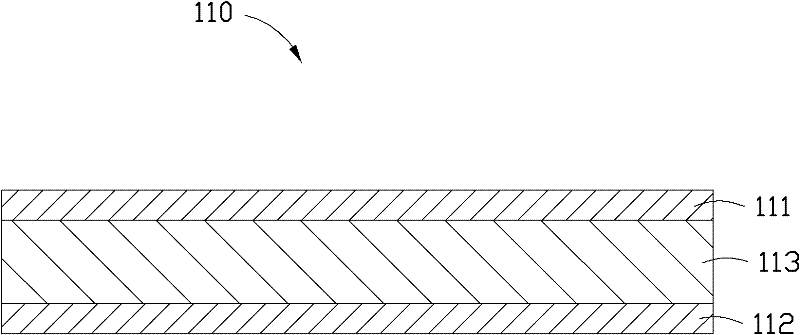
[0042] For a first step, see figure 1 , providing an inner layer substrate 110 .
[0043] In this embodiment, the inner substrate 110 is a double-sided copper-clad board, and the inner substrate 110 includes a first inner conductive layer 111, a second inner conductive layer 112, and a An insulating layer 113 between the inner conductive layers 112 .
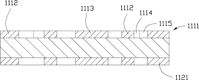
[0044] In the second step, please also refer to the figure 2 The first inner layer conductive layer 111 is formed into a first inner layer circuit pattern 1111 , and the second inner layer conductive layer 112 is fabricated to form a second inner layer circuit pattern 1121 .
[0045] In this embodiment, the first inner conductive layer 11...
PUM
 Abstract
Description
Claims
Application Information