Silicon micro gyroscope with triangular vibrator and manufacturing method thereof
A technology of silicon microgyroscope and manufacturing method, which is applied in the direction of steering induction equipment, etc., can solve the problems of difficult processing of capacitance gap, difficult control of side wall surface roughness precision, easy to cause tunneling, etc., and achieves simple structure, high yield, The effect of simple production process
- Summary
- Abstract
- Description
- Claims
- Application Information
AI Technical Summary
Problems solved by technology
Method used
Image
Examples
Embodiment 1
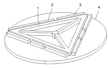
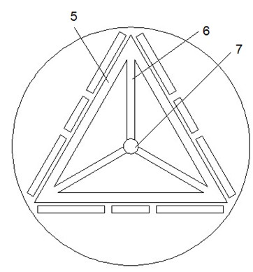
[0035] like figure 1 , figure 2 , image 3 As shown, this embodiment includes an equilateral triangular vibrator 1 with three vibrating beams, a driving electrode 2 parallel to the vibrating beams with a certain gap, a detection electrode 3 parallel to the vibrating beams with a certain gap, and a substrate 4 .
[0036] In this embodiment, the triangular vibrator 1 is composed of three vibration beams 5 connected end to end, three spoke-shaped support beams 6 and a cylindrical support column 7 .
[0037] In this embodiment, there are three driving electrodes 2, which are respectively parallel to the three vibrating beams 5 of the equilateral triangular vibrator 1, and have a certain gap, and are located at the midpoint of the vibrating beams 5. form a capacitor.
[0038] In this embodiment, there are three pairs of detecting electrodes 3 , which are respectively located on both sides of the driving electrode 2 and parallel to the driving beam 5 , and each pair of detecting...
Embodiment 2
[0045] This embodiment relates to the manufacturing process of the microgyroscope described in Embodiment 1, such as Figure 6-Figure 9 As shown, it mainly includes the following steps:
[0046] (a) Clean the silicon wafer, dry it, and then sputter a layer of metal aluminum with a thickness of several microns on the single side of the silicon wafer.
[0047] (b) Using aluminum as a mask, spin-coat a layer of photoresist on the aluminum surface, use the prepared mask to photoresist, develop, then pattern the aluminum mask, and finally use deep reactive ion etching The structure of the driving electrode 2, the detecting electrode 3 and the cylindrical supporting column 7 is deeply etched.
[0048] (c) Remove the aluminum mask in the previous step, clean and dry the silicon wafer, oxidize the cavity etched by the silicon wafer in the previous step, and make a protective layer of silicon oxide to protect the prepared supporting pillars 7 .
[0049] (d) The silicon wafer and ...
PUM
 Abstract
Description
Claims
Application Information


