Multi-layer structure including silicon nanocrystals and method for fabricating photo-sensing unit
A multi-layer structure, silicon nanotechnology, applied in the field of technology
- Summary
- Abstract
- Description
- Claims
- Application Information
AI Technical Summary
Problems solved by technology
Method used
Image

Examples
Embodiment Construction
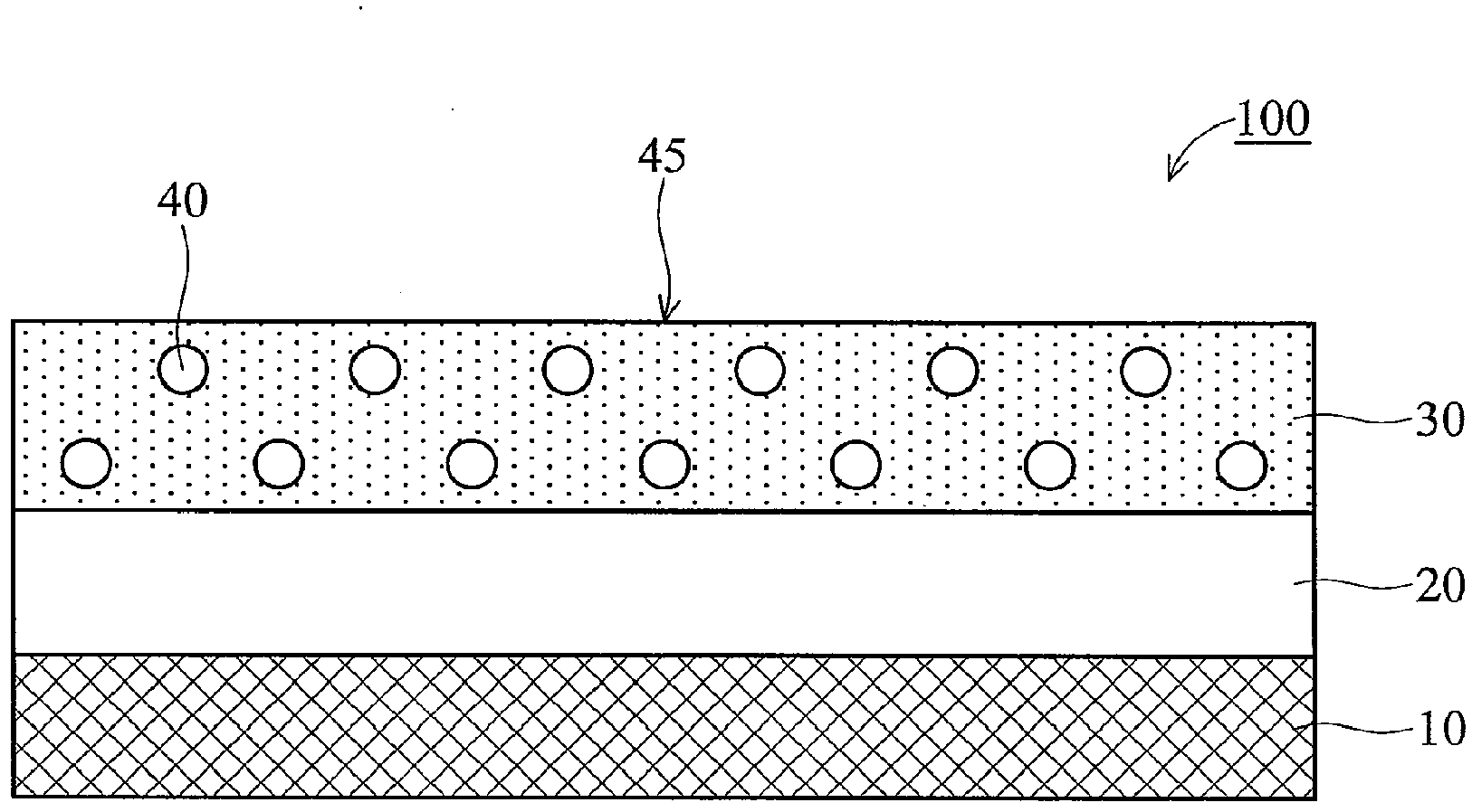
[0109] The following fit figure 1 An embodiment of the present invention fabricated in a multilayer structure including silicon nanocrystals in a silicon-rich dielectric layer is described through FIG. 5 .
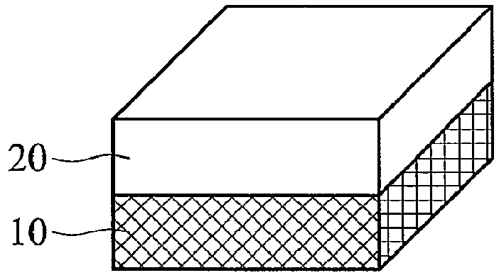
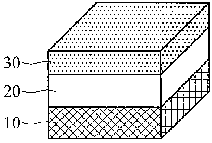
[0110] Please refer to Figure 1 ~ Figure 2D , which describes a multilayer structure 100 comprising silicon nanocrystals 40 in a silicon-rich dielectric layer 30 according to an embodiment of the present invention, figure 1 A cross-sectional view showing a multilayer structure 100 including silicon nanocrystals 40 in a silicon-rich dielectric layer 30, the multilayer structure 100 includes a substrate 10, a first conductive layer 20, a silicon-rich dielectric layer 30, and a silicon-rich dielectric layer A plurality of silicon nanocrystals 40 in 30 . Such as Figure 2D As shown, another conductive layer 50 is formed on the silicon-rich dielectric layer 45 having silicon nanocrystals 40, Figure 3A show Figure 2A-2D A process flow diagram 300 illustrating how the m...
PUM
| Property | Measurement | Unit |
|---|---|---|
| thickness | aaaaa | aaaaa |
| diameter | aaaaa | aaaaa |
| diameter | aaaaa | aaaaa |
Abstract
Description
Claims
Application Information