

Method for manufacturing non-volatile memory and structure thereof
a technology of non-volatile memory and manufacturing method, which is applied in the direction of electrical apparatus, nanotechnology, semiconductor devices, etc., can solve the problems of non-volatile memory already facing a size problem, memory is incapable of maintaining its charging and memory function, and the loss of electrical charges of the memory, so as to achieve no damage to the substrate or other elements
- Summary
- Abstract
- Description
- Claims
- Application Information
AI Technical Summary
Benefits of technology
Problems solved by technology
Method used
Image

Examples
first embodiment
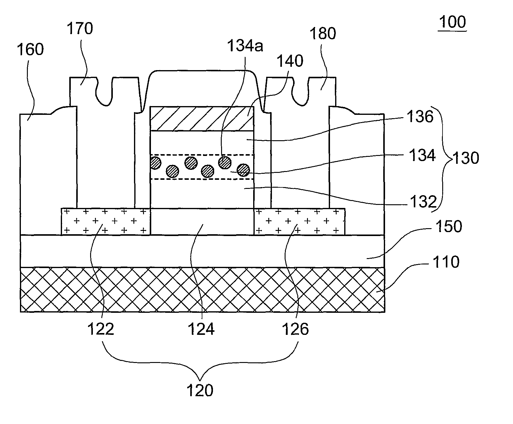
[0023]FIGS. 1˜8 show a method for manufacturing non-volatile memory according to a first embodiment of the invention.
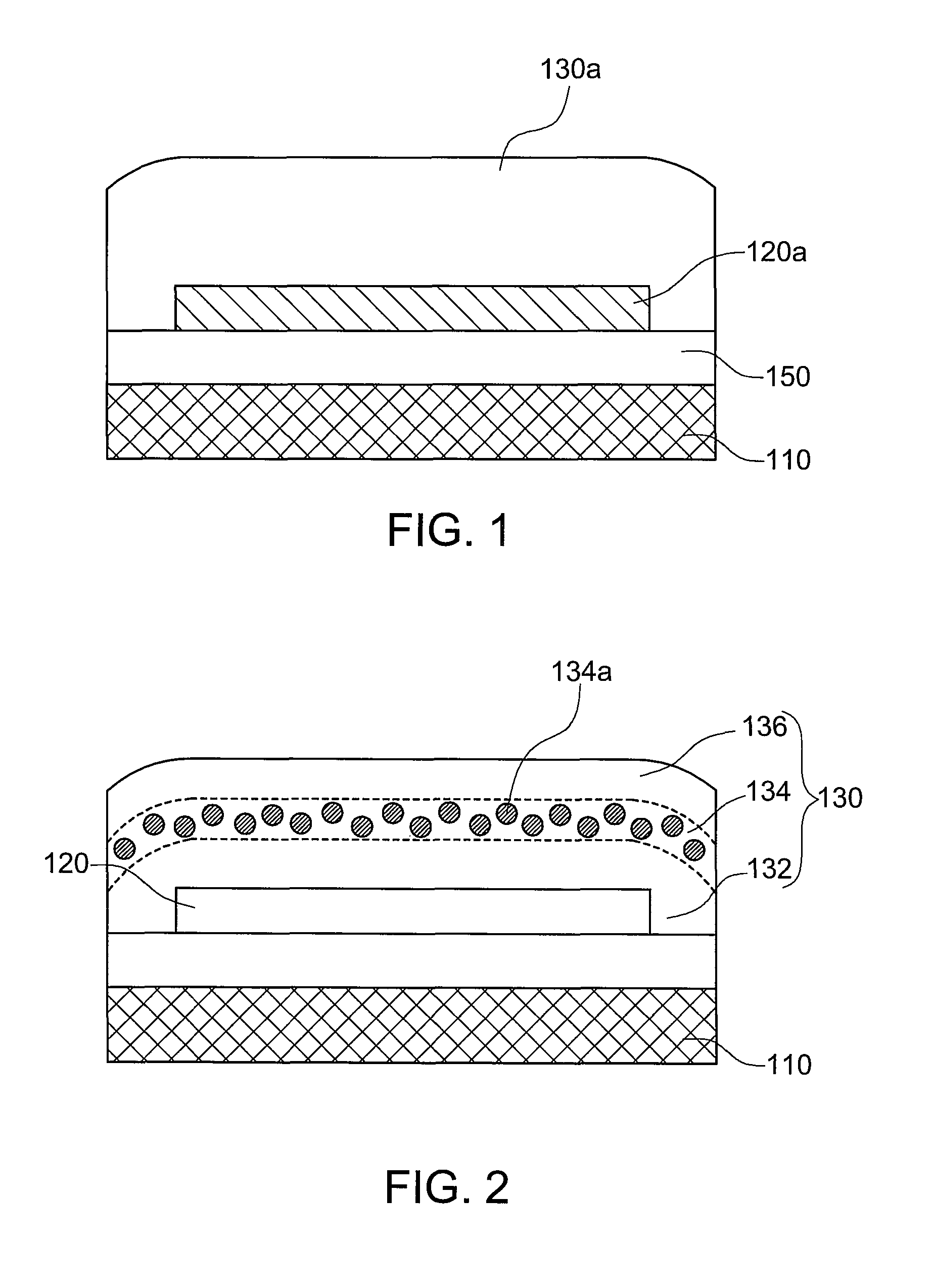
[0024]Referring to FIG. 1. Firstly, a substrate 110 such as Si-substrate, glass substrate or plastic substrate is provided. In the invention, the substrate is exemplified by a glass substrate.
[0025]Next, the present embodiment of the invention preferably comprises the step of forming a buffer layer 150 on the substrate 110. The buffer layer 150, which can be made from a material such as silicon dioxide (SiO2) layer, silicon nitride (Si3N4) layer and amorphous silicon (a-Si) layer, can be formed on the substrate 110 by way of deposition. Thus, the buffer layer 150 can prevent the impurities (such as boron or sodium) of the substrate 110 from being diffused to a semiconductor layer 120 during the subsequent laser annealing process and tarnishing the semiconductor layer 120.
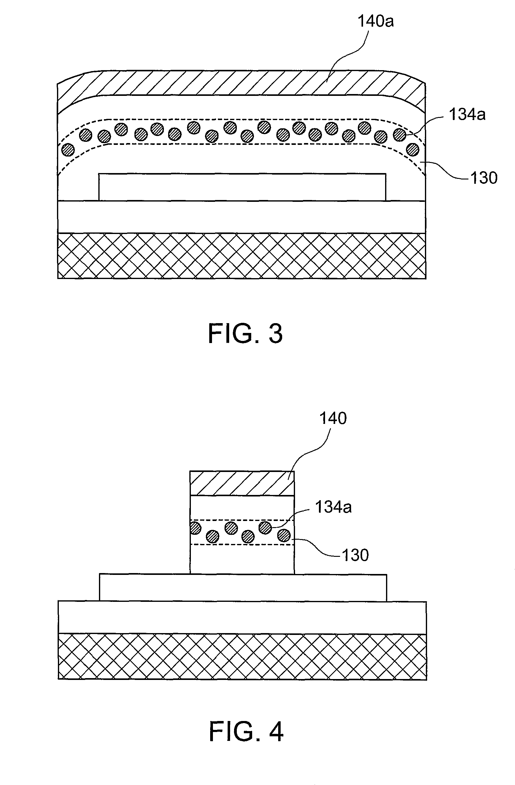
[0026]Next, an a-Si layer 120a is formed on the substrate 110. In the present embodiment of the in...
second embodiment
[0041]Referring to FIG. 10, a method for manufacturing non-volatile memory according to a second embodiment of the invention is shown. The non-volatile memory 200 of the second embodiment differs with the non-volatile memory 100 of the first embodiment only in the structure that the second embodiment preferably has a layer light blocking layer 210 (or a light absorbing layer). The manufacturing method and structure of the second embodiment are similar to that of the first embodiment, and the similarities in terms of structure, material and design conditions are not repeated here.
[0042]As the silicon nanocrystals 134a is very sensitive to the light, the silicon nanocrystals 134a, when absorbing a light, will generate electrical charges and make the stored electrical charges lost or changed. Therefore, in the present embodiment of the invention, the non-volatile memory 200 preferably further comprises a light blocking layer 210 (or a light absorbing layer) made from a light blocking m...
third embodiment
[0043]Referring to both FIG. 8 and FIG. 13. The non-volatile memory 300 of the third embodiment differs with the non-volatile memory 100 of the first embodiment in the structure of the charge storage layer 330 of the third embodiment, and the similarities in terms of structure, material and design conditions are not repeated here.
[0044]FIGS. 11˜13 show a method for manufacturing non-volatile memory according to a third embodiment of the invention.
[0045]Referring to FIG. 11. In the present embodiment of the invention, a tunneling dielectric layer 332 is formed on the a-Si layer 120a of the substrate 110. Next, a Si-rich dielectric layer 334 is formed on the tunneling dielectric layer 332, and then a barrier dielectric layer 336 is formed on the Si-rich dielectric layer 334. In the present embodiment of the invention, the tunneling dielectric layer 332 and the barrier dielectric layer 336 can be made from a material such as silicon dioxide (SiO2), and the characteristics of the materi...
PUM
| Property | Measurement | Unit |
|---|---|---|
| refractive index | aaaaa | aaaaa |
| particle diameter | aaaaa | aaaaa |
| thickness | aaaaa | aaaaa |
Abstract
Description
Claims
Application Information