Normally-off field-controlled channel gan heterojunction diode

A heterojunction, normally-off technology, applied in the direction of electrical components, circuits, semiconductor devices, etc., can solve the problems of poor anti-phase cut-off capability, large forward conduction resistance, and structural incompatibility, etc., and achieve the reduction of field control characteristics, Improved reverse cutoff, low forward voltage drop effect

Inactive Publication Date: 2011-12-14
UNIV OF ELECTRONICS SCI & TECH OF CHINA
View PDF3 Cites 25 Cited by
  • Summary
  • Abstract
  • Description
  • Claims
  • Application Information

AI Technical Summary

Problems solved by technology

[0004] The traditional GaN heterojunction diode (such as SBD) has no field control electrode structure and is a normally-on device with large forward conduction resistance and large power consumption; poor reverse cut-off capability; different from the most mature GaN The AlGaN / GaN HFET structure of the junction switch device is not compatible, which is not conducive to the application of the device

Method used


Image

  • Normally-off field-controlled channel gan heterojunction diode
  • Normally-off field-controlled channel gan heterojunction diode
  • Normally-off field-controlled channel gan heterojunction diode

Examples


Embodiment Construction

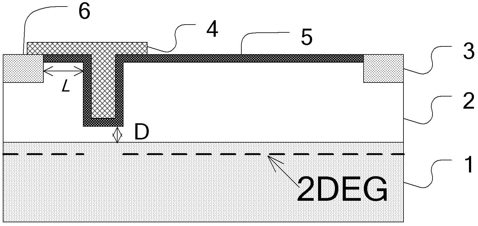
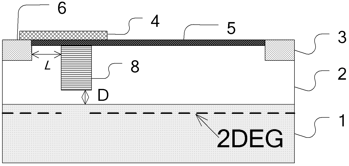
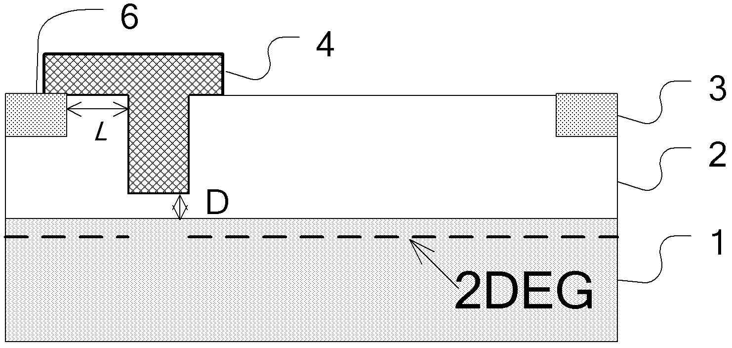
[0031] Normally-off field-controlled channel GaN heterojunction diodes, such as figure 1 , 2 and 7, including: a GaN heterojunction deposited on the substrate surface, a normally-off field-controlled conductive channel, an anode 6 and a cathode 3; the GaN heterojunction is composed of A x Ga 1-x N (A is Al or In, 0x Ga 1-x Between N thin films 2; the normally-off type field-controlled conductive channel includes a two-dimensional electron gas (2DEG) conductive channel at the GaN heterojunction interface and a field-controlled channel located above the GaN heterojunction interface and close to the anode The electrode 4 can realize the on and off of the two-dimensional electron gas conduction channel by controlling the voltage of the field control channel electrode 4; the anode 6 and the cathode 3 are respectively located at the two ends above the GaN heterojunction interface, wherein the anode 6 with A x Ga 1-x The ohmic contact is realized between the N thin films 2 and a...


PUM


Abstract

A normally-off type field-controlled channel GaN heterojunction diode belongs to the technical field of semiconductor devices. The invention adopts the technology of combining insulating layer-groove, modulation doping and groove-modulation doping to change the conductive channel structure of the existing GaN heterojunction diode, and convert the original normally-on spontaneously polarized GaN heterojunction The junction conductive channel is changed into a normally-off field-controlled conductive channel combining spontaneous polarization and piezoelectric polarization in the present invention, which realizes the field-controlled characteristics of the GaN heterojunction diode conductive channel and reduces the forward conduction resistance and enhanced reverse cut-off capability. The invention has lower forward conduction resistance and power consumption, stronger reverse cut-off ability, and is compatible with AlGaN/GaN HEMT power switching device technology, which is beneficial to the application of the device.

Description

technical field [0001] The invention belongs to the technical field of semiconductor devices, and in particular relates to a GaN heterojunction diode. Background technique [0002] Gallium nitride (GaN) is one of the representatives of the third-generation wide-bandgap semiconductor materials, which has the following excellent characteristics: high critical breakdown electric field (~3.5×10 6 V / cm), high electron mobility (~2000cm 2 / V·s), high two-dimensional electron gas (2DEG) concentration (~10 13 cm -2 ), high temperature working ability. GaN-based heterojunction field effect transistors (HFETs) (or high electron mobility HMETs, modulation doped field effect transistors MODFETs, hereinafter collectively referred to as HFETs) have been widely used in the semiconductor field. This type of device has the characteristics of high reverse blocking voltage, low forward conduction resistance, and high operating frequency, so it can meet the system's requirements for semicon...

Claims


Application Information

Patent Timeline
Patent Type & Authority Applications(China)
IPC IPC(8): H01L29/861H01L29/06
Inventor 陈万军张竞汪志刚魏进张波
Owner UNIV OF ELECTRONICS SCI & TECH OF CHINA
Why Eureka
Try Eureka