An Optical Method to Modulate the Persistent Photoconductive Effect of ZnO Nanowires

A zinc oxide nanowire, optical method technology, applied in nanotechnology, nanotechnology, climate sustainability and other directions, to achieve the effect of low cost, convenient method and fast response

Active Publication Date: 2011-12-14
TECHNICAL INST OF PHYSICS & CHEMISTRY - CHINESE ACAD OF SCI
View PDF3 Cites 3 Cited by
  • Summary
  • Abstract
  • Description
  • Claims
  • Application Information

AI Technical Summary

Problems solved by technology

However, a data erasing method suitable for this memory device, that is, a method that can quench

Method used


Image

  • An Optical Method to Modulate the Persistent Photoconductive Effect of ZnO Nanowires
  • An Optical Method to Modulate the Persistent Photoconductive Effect of ZnO Nanowires
  • An Optical Method to Modulate the Persistent Photoconductive Effect of ZnO Nanowires

Examples


Embodiment 1

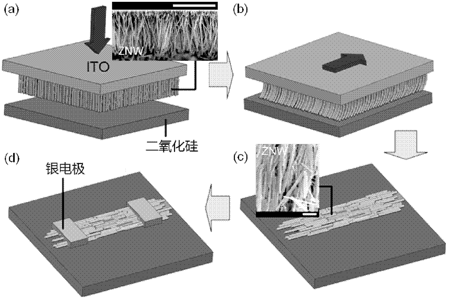
[0013] Electrochemical method is used to prepare zinc oxide nanowires on ITO conductive substrate. The diameter of the prepared zinc oxide nanowires is 50-100nm and the length is 5-10μm, such as figure 1 Inset in (a). Using the zinc oxide nanowire sample, a zinc oxide nanowire optoelectronic device was prepared on a silicon dioxide substrate by "printing method". Specific steps such as figure 1 Shown: (a) The ZnO nanowire array grown on the ITO conductive substrate was lightly placed on the silicon dioxide substrate. The inset is the SEM picture of the ZnO nanowire array, and the scale length is 10 microns; (b) the ZnO nanowire array sample grown on the ITO conductive substrate is drawn across the silicon dioxide substrate along a fixed direction; (c) in two A nanofilm composed of ZnO nanowires with strong directionality is left on the silicon oxide substrate. The inset is the SEM picture of ZnO nanowires arranged in an orderly manner, and the scale length is 1 micron; (d) i...

Embodiment 2

[0016] Referring to Example 1, zinc oxide nanowires were prepared on an ITO conductive substrate by an electrochemical method. The diameter of the prepared zinc oxide nanowires was 50-100 nm and the length was 5-10 μm. Using the zinc oxide nanowire sample, a zinc oxide nanowire optoelectronic device was prepared on a silicon dioxide substrate by "printing method".

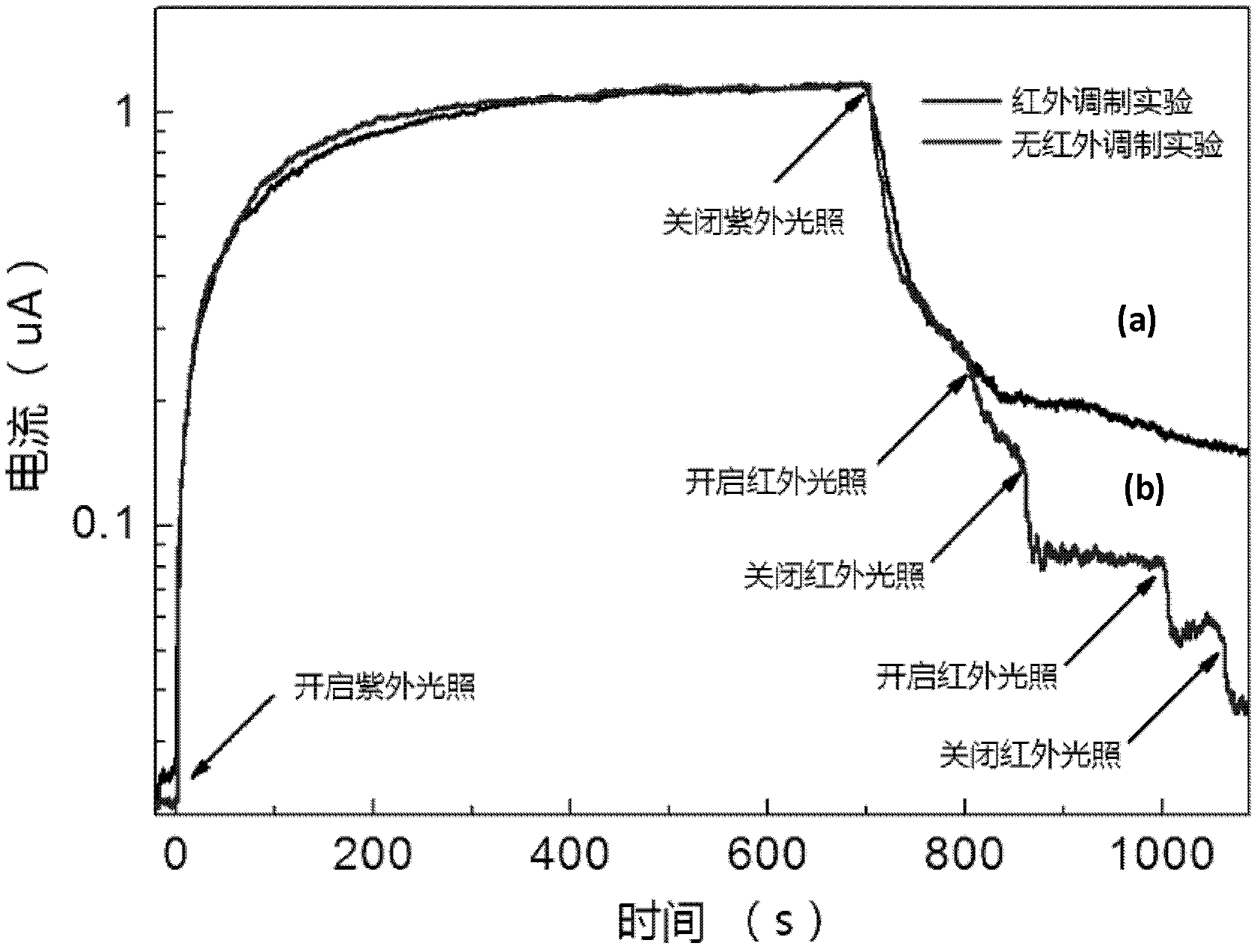
[0017] Apply a voltage of 5V between the two electrodes of the above-mentioned zinc oxide nanowire photoelectric device, use an ultraviolet excitation light source with a wavelength of 365nm to irradiate the zinc oxide nanowire photoelectric device, and then use an infrared light source with a wavelength of 905nm to irradiate the photoelectric device in a continuous photoconductive state. The zinc oxide nanowire optoelectronic device reduces the electrical conductivity of the zinc oxide nanowire optoelectronic device, thereby realizing continuous photoconductive quenching. The effects of ultraviolet and infrared li...

Embodiment 3

[0019] Referring to Example 1, an array of zinc oxide nanowires was prepared on an ITO conductive substrate by an electrochemical method. The diameter of the prepared zinc oxide nanowires was 50-100 nm and the length was 5-10 μm. Using the ZnO nanowire sample, a ZnO nanowire optoelectronic device was prepared on a silicon dioxide substrate by "printing method".

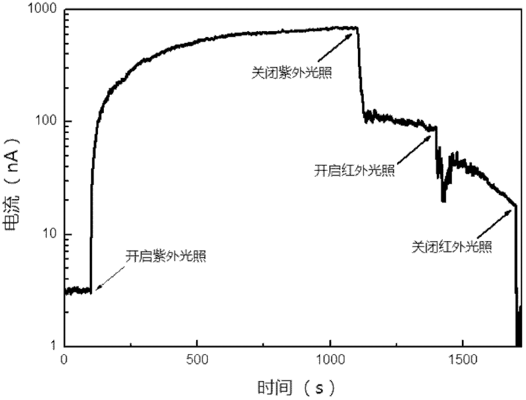
[0020] Apply a voltage of 5V between the two electrodes of the above-mentioned zinc oxide nanowire photoelectric device, use an ultraviolet excitation light source with a wavelength of 365nm to irradiate the zinc oxide nanowire photoelectric device, and then use an infrared light source with a wavelength of 880nm to irradiate the photoelectric device in a continuous photoconductive state. The zinc oxide nanowire optoelectronic device reduces the conductivity of the zinc oxide nanowire optoelectronic device, thereby realizing continuous photoconductive quenching. The effects of ultraviolet and infrared light on the sus...


PUM

PropertyMeasurementUnit
Wavelengthaaaaaaaaaa
Diameteraaaaaaaaaa
Lengthaaaaaaaaaa

Abstract

The invention belongs to the technical field of nanometer material applications, and in particular relates to an optical method for modulating the continuous photoconductive effect of a zinc oxide nanometer wire. According to the invention, a photoelectric device of the zinc oxide nanometer wire under the continuous photoconduction state is irradiated by utilizing infrared light, and the electricconductivity of the photoelectric device of the zinc oxide nanometer wire is reduced, thus the quenching of continuous photoconduction is realized. According to the invention, after a nonvolatile optical memory based on the zinc oxide nanometer wire is subjected to excitation by ultra violet irradiation, the nonvolatile optical memory under the continuous photoconduction state is irradiated by the infrared light, and the electric conductivity of the nonvolatile optical memory is reduced, thus the erasure of data is realized. The method provided by the invention has the advantages of repaid response and low cost, is convenient and rapid, and is especially suitable for the applications of the nonvolatile optical memory based on the zinc oxide nanometer wire.

Description

technical field [0001] The invention belongs to the technical field of nanometer materials application, in particular to an optical method for modulating the continuous photoconductive effect of zinc oxide nanowires. Background technique [0002] Recently, with the increasing application of ZnO one-dimensional nanomaterials in optoelectronic devices, the phenomenon of persistent photoconductivity (PPC) based on ZnO one-dimensional nanomaterials has also been frequently reported (Hullavarad et al.2009, Nanoscale Research Letters 4(12):1421-1427.; Liao, Lu et al.2009, Applied Physics a-Materials Science & Processing 95(2):363-366; Liu, She et al.2009, Applied Physics Letters 94(6) :063120). The persistent photoconductivity phenomenon refers to the phenomenon that the semiconductor material in the excited state can still maintain a high conductance state for a long time even when the excitation light source is lost. This is not quite consistent with the photoresponse of ordin...

Claims


Application Information

Patent Timeline
IPC IPC(8): H01L31/18B82Y10/00
CPCY02P70/50
Inventor 师文生王耀佘广为
Owner TECHNICAL INST OF PHYSICS & CHEMISTRY - CHINESE ACAD OF SCI
Why Eureka
Try Eureka