A light emitting diode and its manufacturing method

A technology of light-emitting diodes and manufacturing methods, applied in semiconductor/solid-state device manufacturing, light sources, electric light sources, etc., can solve the problems of nuts not being tightly fitted, poor heat dissipation of brackets, and complicated assembly processes, etc., to achieve convenient thermal design, light The effect of full shape and improved light output efficiency

Inactive Publication Date: 2011-12-14
曲丹
View PDF1 Cites 5 Cited by
  • Summary
  • Abstract
  • Description
  • Claims
  • Application Information

AI Technical Summary

Problems solved by technology

[0003] At present, the power LEDs on the market are mainly based on the surface-mount structure, which is to fix one or several light-emitting chips on a flat substrate. Since the light-emitting angle of the chip itself will not exceed 180 degrees, this surface-mount structure is limited by the chip. Due to the influence of its own angle and the light blocking effect of the flat substrate, the maximum luminous angle of LEDs with this structure will not exceed 180°, and there is a defect that the lighting angle is limited. Therefore, when LEDs with this structure want to replace incandescent bulbs and are used in general lighting, they must be Many of them are assembled into a three-dimensional module to make the light angle break through 180° before it can be used
There is another kind of three-dimensional luminous 360-degree light source (Chinese patent application number: 200780019635.4, invention name: semiconductor light source for physical space lighting with three-dimensional bracket), which can achieve three-dimensional luminous effect, but its own structure design determines its The light efficiency is low. Many chips are solidified on the cathode, and only rely on the cathode to dissipate heat. Secondly, the threaded structure on the bracket cannot fit closely with the nut on the heat sink in actual lighting, and the actual contact area with the heat sink is not large. Therefore, the heat dissipation effect of the bracket itself is poor, resulting in poor lighting effect. In addition, there are many components and the assembly process is relatively complicated, so its industrialization is difficult.

Method used


Image

  • A light emitting diode and its manufacturing method
  • A light emitting diode and its manufacturing method
  • A light emitting diode and its manufacturing method

Examples


Embodiment Construction

[0041] The specific implementation manners of the present invention will be described in detail below in conjunction with the accompanying drawings of the embodiments.

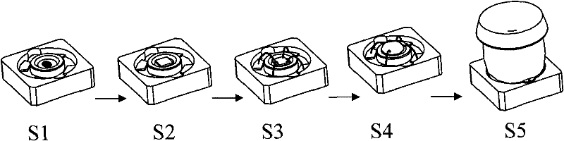
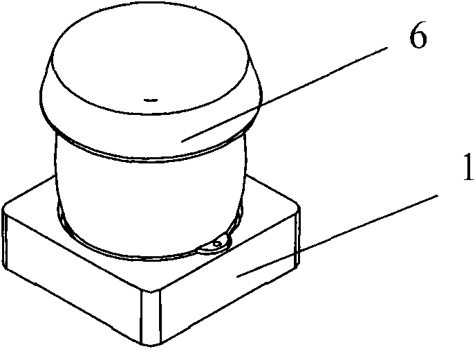
[0042] see figure 1 , see also Figure 2-Figure 4 . As shown in the figure, the manufacturing procedure of the light-emitting diode of the present invention is as follows:

[0043] S1, glue dispensing step, using equipment to directly point high thermal conductivity glue 2 (such as silver glue or solder paste) onto the carrier 1 . Under special requirements (such as the preparation of a higher-power light-emitting diode), eutectic soldering or flip-chip technology can be used, and this step can be omitted.

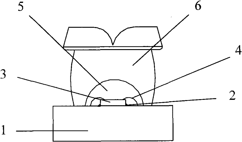
[0044] S2, crystal-bonding step, see also figure 2, the carrier 1 is a material with high thermal conductivity (it can be insulated, or it can be a conductor), and its composition can be a ceramic substrate, a combination bracket of PPA and metal columns, a metal PCB board, etc. The middle of the carr...


PUM


Abstract

A light-emitting diode and a manufacturing method thereof relate to a light source structure, which solves the problem that the light-emitting angle of the existing LED cannot exceed 180° at most, and the lighting angle is limited. The light-emitting diode of the present invention uses high thermal conductivity glue on the carrier. One or more light-emitting chips are fixedly connected; the carrier and the light-emitting chip are electrically connected with wires, so that the carrier and the light-emitting chip become a semi-finished light-emitting diode; The invention utilizes the lens to condense the light of the light-emitting chip first, then refracts and scatters the light, so that the light shape is fuller and has a 3D light-emitting effect. The good heat dissipation structure and the popularization of the production process make the yield rate (99%) higher, which greatly reduces the manufacturing cost of the product.

Description

technical field [0001] The invention relates to a structure of a light source, in particular to a structure of a light emitting diode with a 3D light emitting effect. Background technique [0002] Light-emitting diodes (LEDs), as the fourth generation of lighting energy, have highlighted their advantages in landscape, indication, display, backlight and special lighting applications, and have already exerted great effects such as energy saving, longevity, and fast response. In the 100-year history of the development of lighting technology, the development of LED has only been a few decades, and the application of low-power light-emitting diodes has always been the main application. Because LED has the characteristics of easy dynamic control of brightness and color, small size, long life, no infrared and ultraviolet rays in the beam, and strong luminous directionality, it has entered the field of general lighting on a large scale. However, in order to give full play to the pe...

Claims


Application Information

Patent Timeline
Patent Type & Authority Applications(China)
IPC IPC(8): H01L33/48H01L33/58H01L33/64H01L21/50H01L25/075F21S2/00F21Y101/02
CPCH01L2224/48091H01L2224/48247
Inventor 曲丹段国友卞长友
Owner 曲丹
Why Eureka
Try Eureka