Bonded wafer with thermal stress relief structure and laser scribing process

A technology of laser scribing and thermal stress, which is applied in the field of laser scribing process and bonded wafers, and can solve the problems of limiting the application of invisible laser scribing process, complex bonded wafer scribing process, and difficulty in free-form scribing. , to achieve the effects of improved mechanical properties, high yield, and reduced scribing costs

Active Publication Date: 2011-12-21
NAT UNIV OF DEFENSE TECH
View PDF2 Cites 8 Cited by
  • Summary
  • Abstract
  • Description
  • Claims
  • Application Information

AI Technical Summary

Problems solved by technology

However, when the bonded wafer is diced using the stealth laser scribing process, it is necessary to use lasers with different wavelengths for scribing each layer of different material wafers, which makes the bonded wafer scribing process complicated. The equipment investment is expensive, and the dicing cost has increased sharply [Y. Izawa, S. Tanaka, H. Kikuchi, "Debris-free In-air Laser Dicing for Multi-layer MEMS by Perforated Internal Transformation and Thermally-induced Crack Propagation", MEMS 2008 , Tucson, AZ, USA, January 13-17, 2008, pp.822-827.]
Moreover, for the invisible laser scribing process, it is quite difficult to complete free-form scribing, which limits the application of the invisible laser scribing process

Method used


Image

  • Bonded wafer with thermal stress relief structure and laser scribing process
  • Bonded wafer with thermal stress relief structure and laser scribing process
  • Bonded wafer with thermal stress relief structure and laser scribing process

Examples


Embodiment 1

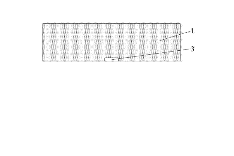
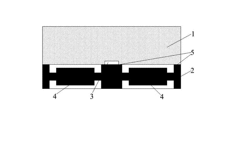
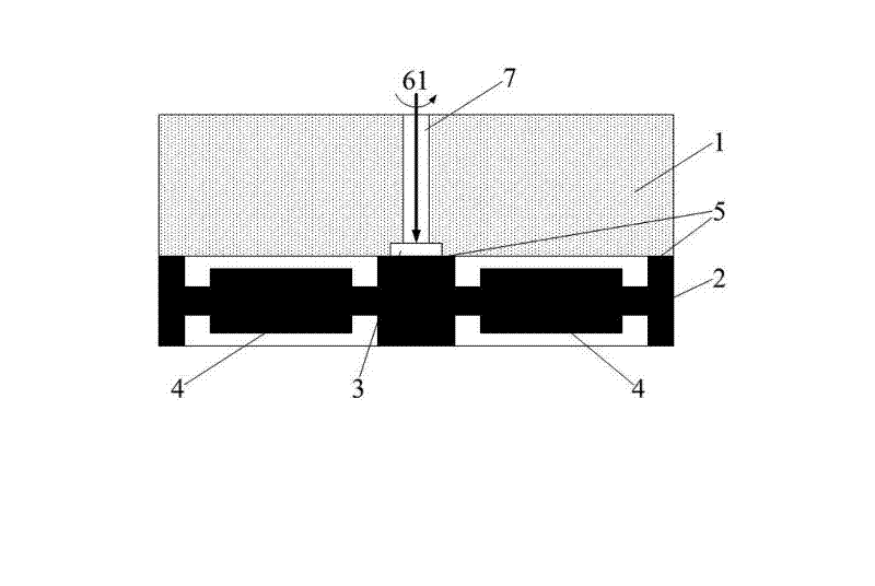
[0043] Such as figure 2 As shown, a bonded wafer with a thermal stress relief structure of the present invention is a double-layer wafer structure, including a glass wafer 1 and a silicon wafer 2 that are bonded to each other, and on the lower surface of the glass wafer 1 On the side close to the bonding contact surface 5, a thermal stress relief structure is correspondingly provided along the planned laser scribing track, and a certain number of MEMS silicon microstructures 4 are fabricated on the silicon wafer 2; in this embodiment, the thermal stress relief The structure is a thermal stress relief groove 3, which is set on the glass wafer 1 close to the bonding contact surface 5, the width of the thermal stress relief groove 3 is larger than the width of the proposed laser scribing track, and the thermal stress relief groove 3 The depth is 8 microns.

[0044] A laser scribing process such as Figure 1 ~ Figure 4 As shown, it specifically includes the following process st...

Embodiment 2

[0050] Such as Figure 6 As shown, a bonded wafer with a thermal stress relief structure of the present invention, the structure of the bonded wafer in this embodiment is basically the same as that of Embodiment 1, the difference is that the thermal stress relief groove 3 is opened in the silicon piece on wafer 2.

[0051] A laser scribing process such as Figure 5 ~ Figure 8 As shown; the laser scribing process of this embodiment is basically the same as that of Embodiment 1, only differing in the processing of the thermal stress relief structure in step (1). This embodiment utilizes a dry etching process to release the thermal stress relief groove 3 Found on silicon wafer 2, see Figure 5 ; Then, complete the scribing process through the same bonding double-layer wafer step and laser scribing step as in Example 1, see Figure 6 ~ Figure 8 .

[0052] After the dicing is completed, it can be seen from the scanning electron microscope image of the dicing cut section of the ...

Embodiment 3

[0054] Such as Figure 10 As shown, a bonded wafer with a thermal stress relief structure of the present invention is a three-layer wafer structure, which includes a top glass wafer 11, a silicon wafer 2 and a bottom that are bonded to each other from top to bottom. A certain amount of MEMS silicon microstructures 4 are made on the glass wafer 12 and the silicon wafer 2. On the top glass wafer 11, a side close to the top bonding contact surface 51 is correspondingly provided with a top heat sink along the planned laser scribing track. The stress relief groove 31, the silicon wafer 2 is located between two glass wafers, and the side of the bottom glass wafer 12 close to the bottom bonding contact surface 52 is correspondingly provided with bottom thermal stress relief along the planned laser scribing track Groove 32, the width of top thermal stress relief groove 31 and bottom thermal stress relief groove 32 is greater than the width of the proposed laser scribing track, and the...


PUM

PropertyMeasurementUnit
depthaaaaaaaaaa

Abstract

The invention discloses a bonded wafer with a thermal stress release structure. The bonded wafer comprises a glass wafer and a silicon wafer which are jointed with each other; a thermal stress release structure for laser scribing is arranged at the position close to a bonding contact surface of the bonded wafer; the thermal stress release structure is correspondingly arranged along a drafted laser scribing track; the stress release structure of the bonded wafer provided by the invention can prevent an original bonding region close to the scribing track from cracking, improve the laser scribing yield of the bonded wafer and reduce the scribing cost. The invention further discloses a laser scribing process; the laser scribing process comprises a thermal stress release structure process step, bonding wafer and laser scribing processing steps and the like; the laser scribing process can effectively release the thermal stress in the process of laser scribing so as to inhibit a thermal crack on a bonding contact surface, the mechanical property of the bonding contact surface is greatly improved, which is beneficial to the improvement of the MEMS (micro-electromechanical system) chip property; meanwhile, the process is simple and mature and can guarantee lower cost and higher yield.

Description

technical field [0001] The invention mainly relates to the field of micromachining (MEMS), in particular to a bonded wafer with a thermal stress release structure and a laser scribing process. Background technique [0002] As more and more MEMS devices are manufactured on bonded wafers, the dicing process of bonded wafers has become a key process that affects the yield of MEMS devices. At present, the commonly used bonded wafer scribing processes mainly include mechanical scribing and laser scribing. The mechanical scribing process needs to use coolant to cool the grinding wheel, which will introduce pollutants and affect the cleanliness of MEMS device chips, so it is rarely used for dicing bonded wafers; use laser beams for non-contact processing Laser scribing has gradually become the mainstream process for bonded wafer scribing due to its advantages of high precision, high efficiency and no pollution. [0003] Currently, the commonly used ablation laser dicing process (...

Claims


Application Information

Patent Timeline
Patent Type & Authority Applications(China)
IPC IPC(8): B81B7/00B81C1/00B23K26/40B23K26/42B23K26/38B23K26/402B23K26/60
Inventor 吴学忠肖定邦陈志华张旭胡小平侯占强周泽龙
Owner NAT UNIV OF DEFENSE TECH
Why Eureka
Try Eureka