New ic packaging manufacturing process

A manufacturing process and packaging process technology, applied in the field of IC packaging process, can solve the problems of easily changing cover plates, low packaging precision, and uneven etching lines, etc., and achieve the effect of neat shape edges and high line precision.

Inactive Publication Date: 2011-12-21
慈溪市永旭丰泰电子科技有限公司
View PDF0 Cites 9 Cited by
  • Summary
  • Abstract
  • Description
  • Claims
  • Application Information

AI Technical Summary

Problems solved by technology

[0004] The purpose of the present invention is to provide a new type of IC packaging manufacturing process. The process steps are rigorous and the method is scientific, which solves the problem of IC packaging in the prior art that the packaging accuracy is not high due to the rough etching lines and the easy change of the cover plate. and poor sealing

Method used


Image

  • New ic packaging manufacturing process
  • New ic packaging manufacturing process

Examples


Embodiment Construction

[0046] The present invention is described in further detail below:

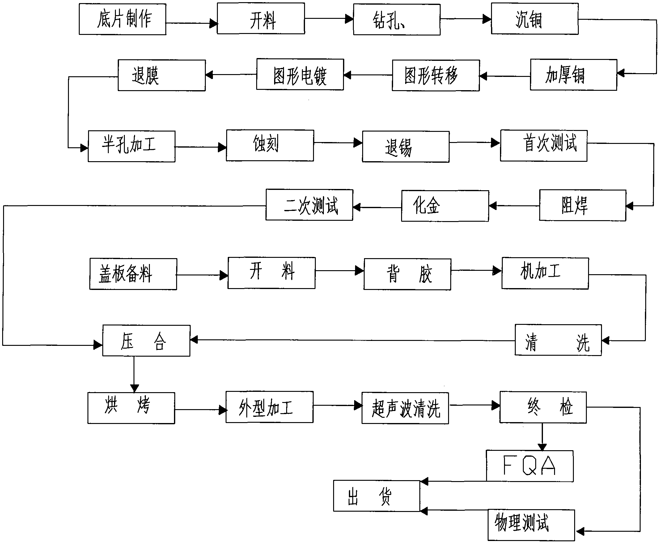
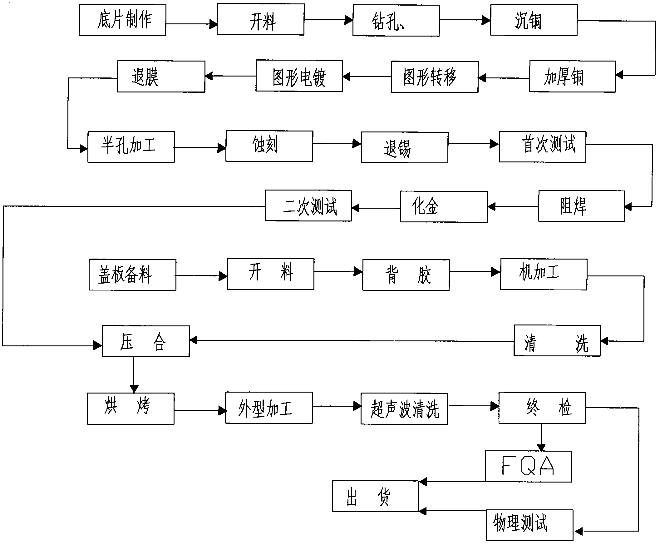
[0047] Such as figure 1 As shown, a new type of IC packaging manufacturing process, including the bottom film manufacturing process, the cover plate manufacturing process and the packaging process of the bottom film and the cover plate,

[0048] Described film manufacturing process comprises:

[0049] Step 1.1, negative film production, that is, the production of light-painted negative film; process compensation must be carried out when performing light-painted negative film, and the process compensation must be determined based on measuring the side etching of Cu with different thicknesses. The negative film is a positive film, and the line width compensation method Yes: formula [loss amount (MIL) = base copper (MIL) / 1.2], for example: 35UM base copper has a loss amount of 35 / 25.4*1.2=1.2miL, and its loss amount is line width loss amount + compensation amount, The line width can be adjusted within the requ...


PUM


Abstract

A new type of IC packaging manufacturing process, including the back plate manufacturing process, the cover plate manufacturing process and the packaging process of the back plate and the cover plate, wherein the back plate manufacturing process includes film production; material cutting; drilling; sinking copper; thickening copper; pattern transfer ;Graphic electroplating; Stripping film; Half-hole processing; Etching; Stripping tin; Solder mask; Gold plating; Cover plate manufacturing process includes cover plate preparation; The process includes pressing; baking; cleaning; final inspection. The beneficial effects of the present invention are: the manufactured lines have high precision, no residual copper and smooth lines after etching, no deformation of the cover plate, no serious glue overflow, the bonding force between the cover plate and the main board reaches more than 10KG, and the substrate has no separation after machining. Layers, half holes without burrs, neat edges and no dust.

Description

technical field [0001] The invention relates to an IC packaging technology, in particular to a novel IC packaging technology. Background technique [0002] IC packaging refers to connecting the circuit pins on the silicon chip to the external joints with wires so as to connect with other devices. The packaging form refers to the shell used to install the semiconductor integrated circuit chip. It not only plays the role of installing, fixing, sealing, protecting the chip and enhancing the electrothermal performance, but also connects the contacts on the chip to the pins of the package shell with wires, and these pins pass through the wires on the printed circuit board. Connect with other devices to realize the connection between the internal chip and the external circuit. Because the chip must be isolated from the outside world to prevent the acrobatics in the air from corroding the chip circuit and causing electrical performance degradation. [0003] There are many types o...

Claims


Application Information

Patent Timeline
Patent Type & Authority Applications(China)
IPC IPC(8): H01L21/50H01L21/60H01L21/56
Inventor 陈胜华
Owner 慈溪市永旭丰泰电子科技有限公司
Why Eureka
Try Eureka