Process for producing semiconducting layers and coated substrates, in particular planar substrates, treated with elemental selenium and/or elemental sulfur

A semiconductor and elemental sulfur technology, applied in semiconductor/solid-state device manufacturing, semiconductor devices, coatings, etc., can solve problems such as toxicity, and achieve high safety, low risk treatment, and low economic cost

Inactive Publication Date: 2015-08-05
PROBST VOLKER (I) (DE)
View PDF2 Cites 0 Cited by
  • Summary
  • Abstract
  • Description
  • Claims
  • Application Information

AI Technical Summary

Problems solved by technology

Furthermore, due to the toxicity and explosiveness of these gases, the safety risks to produ

Method used


Image

  • Process for producing semiconducting layers and coated substrates, in particular planar substrates, treated with elemental selenium and/or elemental sulfur
  • Process for producing semiconducting layers and coated substrates, in particular planar substrates, treated with elemental selenium and/or elemental sulfur
  • Process for producing semiconducting layers and coated substrates, in particular planar substrates, treated with elemental selenium and/or elemental sulfur

Examples


Embodiment Construction

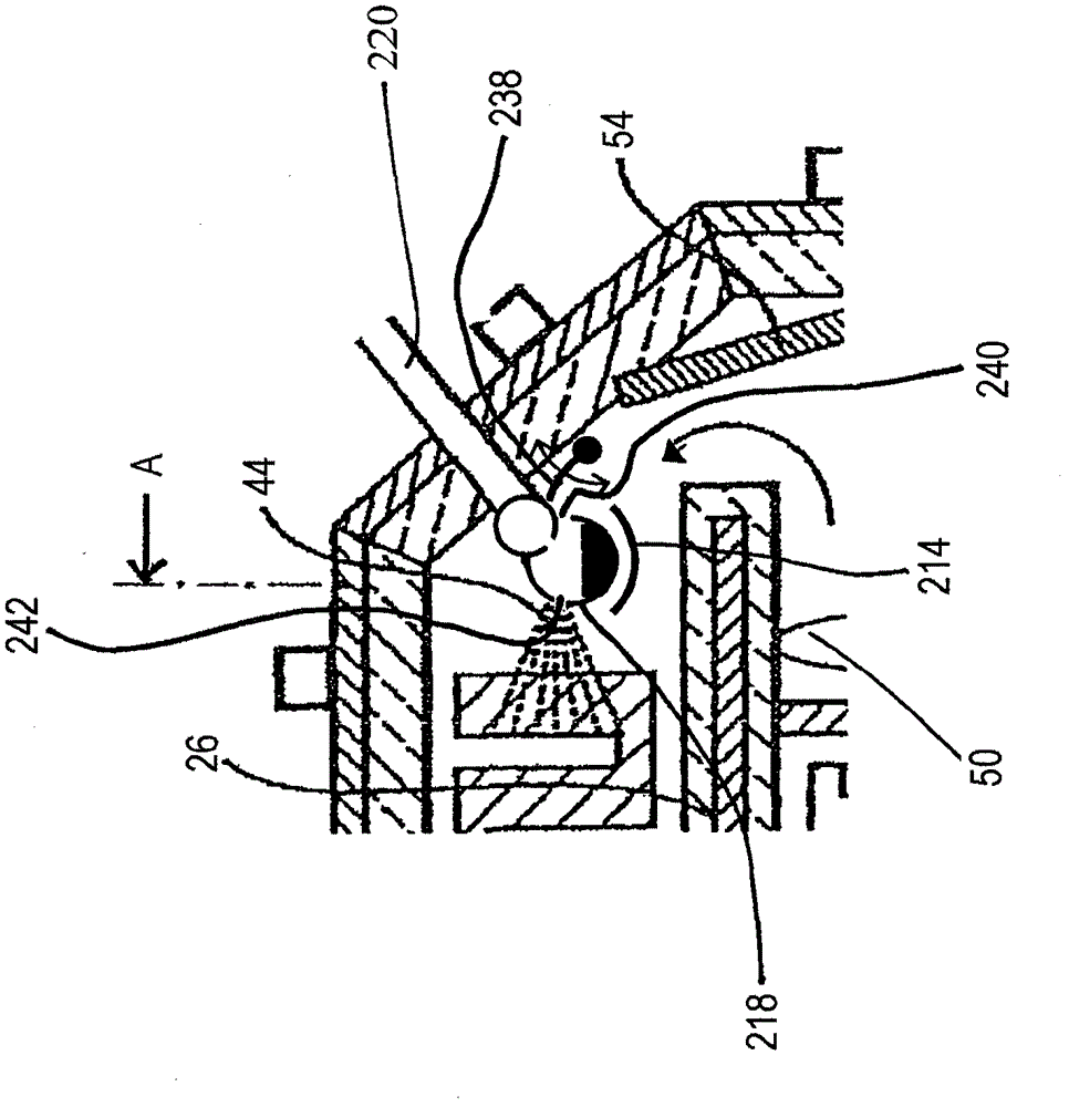
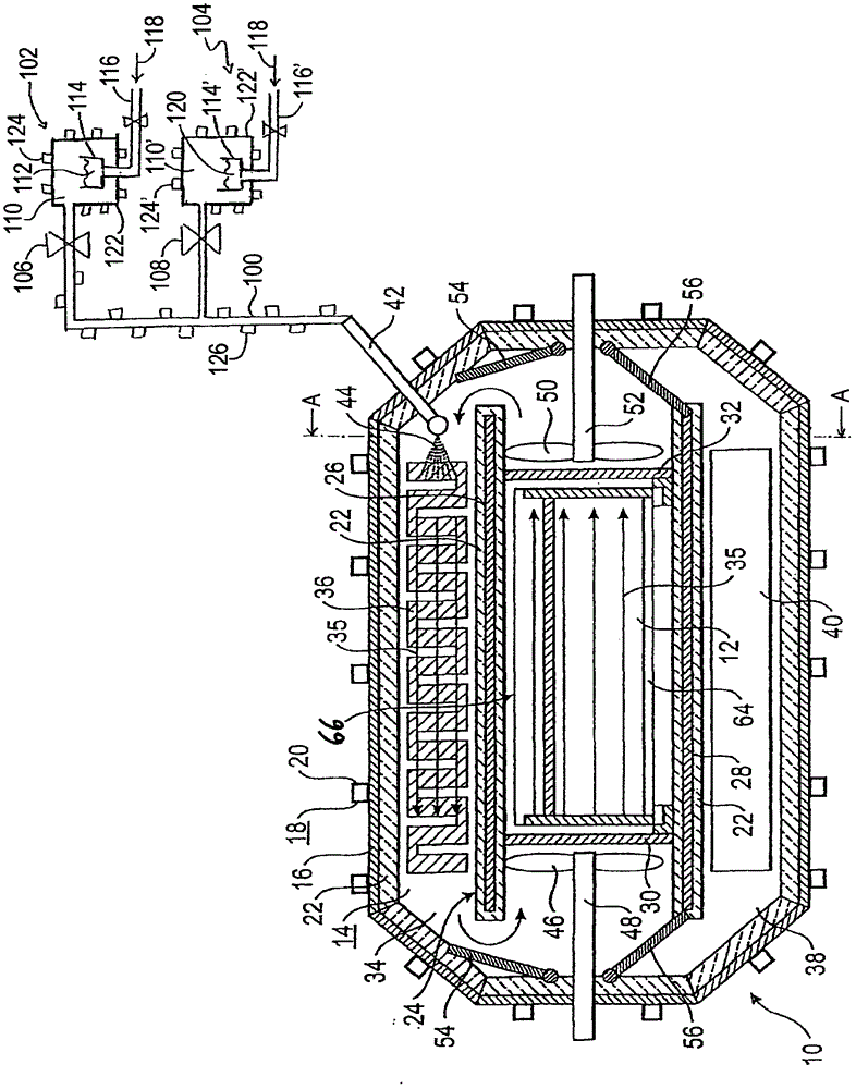
[0088] figure 1 shows a processing device 10 according to the invention designed for the formation of Cu(In,Ga)(Se,S) on a substrate 12 for the production of solar cells 2 Thin layer of semiconductor.

[0089] The processing device 10 comprises an evacuatable processing chamber 14 delimited by processing chamber walls 16 . The chamber wall 16 is made of stainless steel and is kept at a temperature in the range of 150° C. to 250° C. by means of a tempering device 18 .

[0090] In this exemplary embodiment, the tempering device 18 is formed by a duct 20 which is attached to the outside of the treatment chamber 14, in particular may be welded to the treatment chamber wall 16, and which is arranged meanderingly around the treatment chamber 14, at A suitable thermal oil flows in the conduit 20 . Alternatively or additionally, hot oil may also flow through channels (not shown) suitably inserted into the process chamber wall 16 . Furthermore, the outer side of the chamber wall 16...


PUM


Abstract

A processing device for producing semiconductor layers and coated substrates treated with elemental selenium and/or sulphur includes an evacuable processing chamber for receiving a substrate to be processed. The substrate has a metal layer and/or a layer containing metal. A heating device provides convective heating of the substrate to a predetermined temperature. A first source of elementary selenium and/or sulphur vapor is located outside the processing chamber and connected to the processing chamber via a first feed line and/or a second source of elementary selenium and/or sulphur vapor is located inside the processing chamber. The elementary selenium and/or sulphur vapor is guided past the metal layer and/or layer containing metal, chemically reacting said layer with selenium or sulphur in a targeted manner. The substrate is heated and the elementary selenium and/or sulphur vapor is mixed and guided past the substrate by forced convection of a gas conveying device.

Description


Claims


Application Information

Patent Timeline
Owner PROBST VOLKER (I) (DE)
Why Eureka
Try Eureka