Magnetic random access memory cell array, memory and reading/writing method thereof
A random access memory, random storage technology, applied in static memory, digital memory information, information storage and other directions, can solve the problem that MRAM array cannot provide Rashba storage unit read and write separation mechanism, cannot effectively support Rashba storage unit read and write operations, devices The problem of high working noise, etc., achieves the effect of fewer production processes, increased data writing speed, and reduced device power consumption
- Summary
- Abstract
- Description
- Claims
- Application Information
AI Technical Summary
Problems solved by technology
Method used
Image

Examples
Embodiment 1
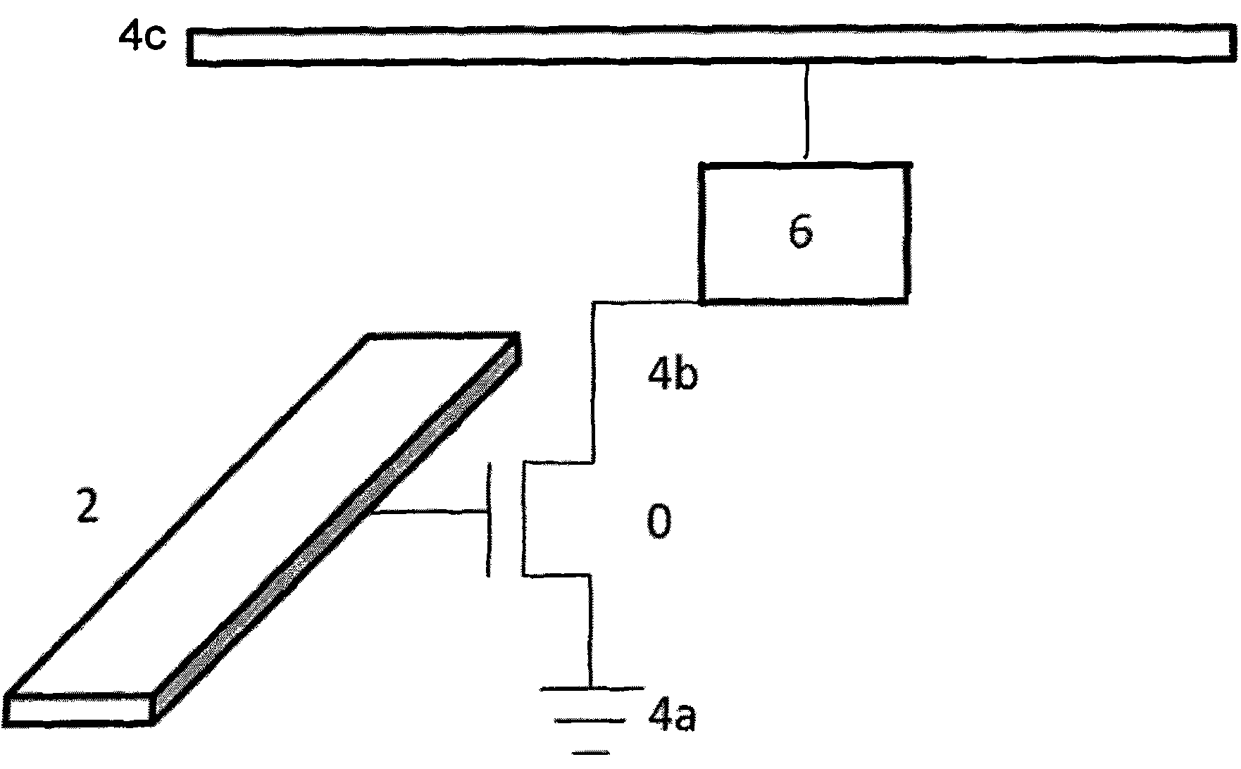
[0066] According to Embodiment 1 of the present invention, a magnetic random access memory (MRAM) array based on the Rashba effect is provided. FIG. 2(a) exemplarily shows a planar wiring diagram of a 2×2 memory cell array. With reference to Fig. 2 (a), this 2 * 2 storage cell array can realize larger-scale two-dimensional storage array along X, Y direction expansion, if this planar array is along Z direction (that is, perpendicular to X, the plane that Y constitutes The direction of) expansion can realize three-dimensional storage array. The bottom layer of each memory cell occupies a transistor T, and in this embodiment, two transistors T share a source. From the perspective of actual device technology, the MRAM array needs to be prepared layer by layer (generally, layer by layer from bottom to top). In this embodiment, the functional units of the MRAM array are distributed on the first to sixth layers. The specific layout design of this embodiment will be described below ...
Embodiment 2
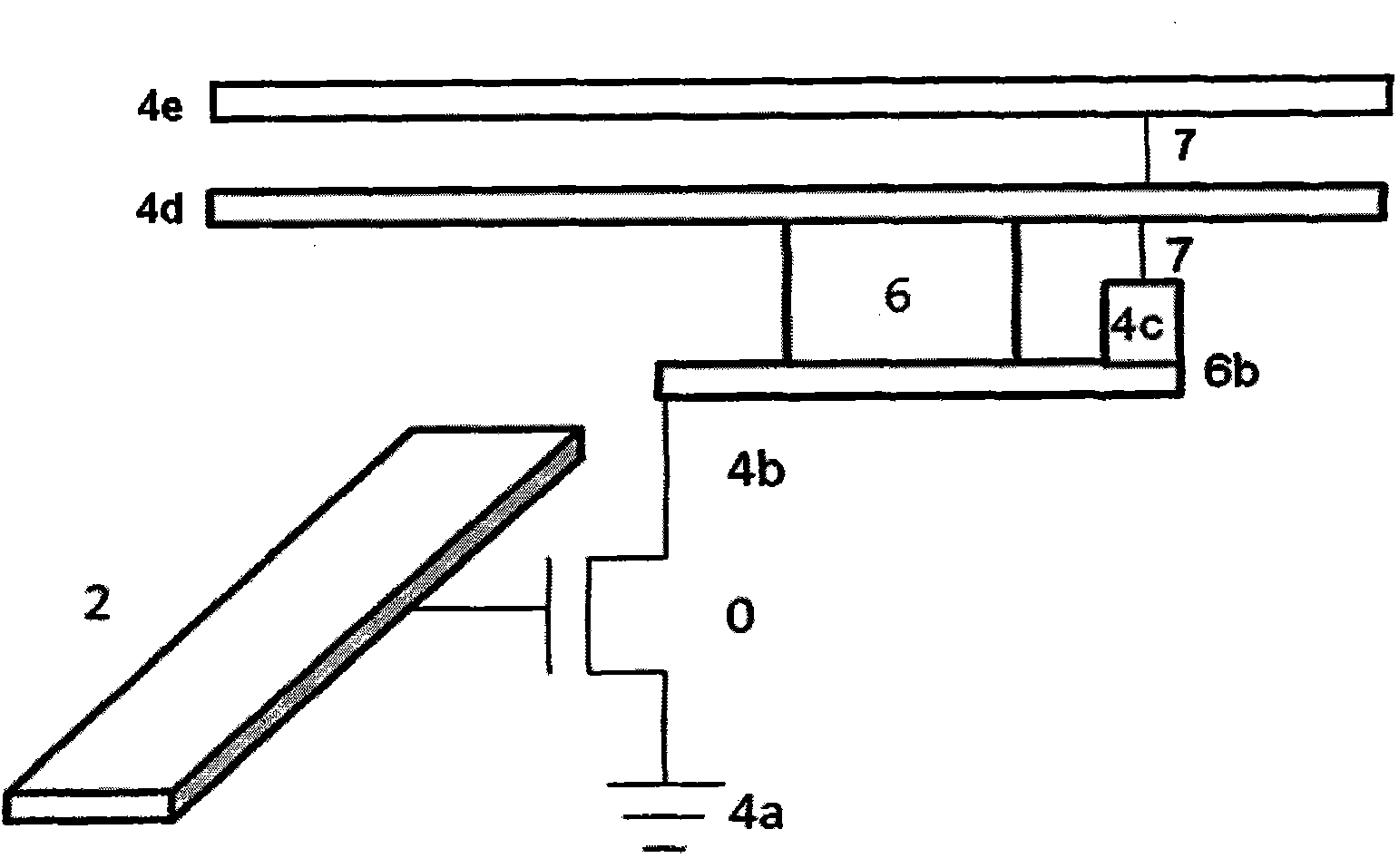
[0082] According to Embodiment 2 of the present invention, a magnetic random access memory (MRAM) array based on the Rashba effect is provided. FIG. 3(a) exemplarily shows a planar wiring diagram of a 2×2 memory cell array. With reference to Fig. 3 (a), this 2 * 2 storage cell array can realize larger-scale two-dimensional storage array along X, Y direction expansion, if this planar array is along Z direction (that is, perpendicular to X, the plane that Y constitutes The direction of) expansion can realize three-dimensional storage array. The bottom layer of each memory cell occupies a transistor T, and in this embodiment, two transistors T share a source. From the perspective of actual device technology, the MRAM array needs to be prepared layer by layer (generally, layer by layer from bottom to top). In this embodiment, the functional units of the MRAM array are distributed on the first to fifth layers. The specific layout design of this embodiment will be described below ...
Embodiment 3
[0092] According to an embodiment of the present invention, an MRAM memory is provided, and the MRAM memory includes an MRAM memory cell array and a read / write circuit. Wherein, the MRAM memory cell array can be the MRAM memory cell array described in Embodiment 1 or 2.
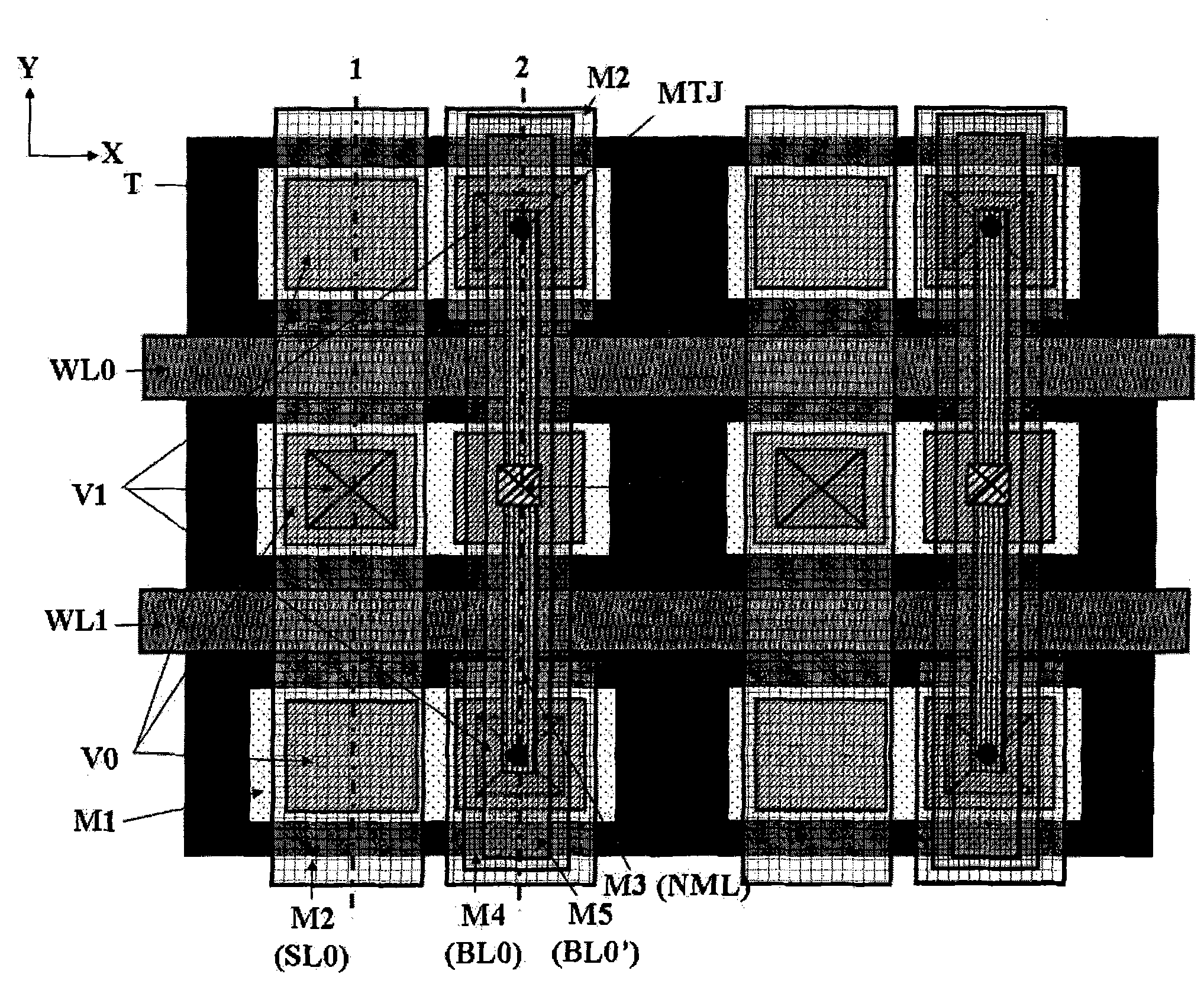
[0093] Such as Figure 4A As shown, this embodiment provides a read-write circuit based on the memory array of Embodiment 1 or 2. Figure 4A Among them, BL is the abbreviation of BitLine (bit line), and the letter x represents the number 0, 1, 2, 3...etc., BLx represents BL0, BL1, BL2, BL3,..., BL15 equipotential lines. Similarly, BLx' stands for BL0', BL1', BL2', BL3',..., BL15' equipotential line, SL is the abbreviation of SourceLine (source line), SLx stands for BL0, BL1, BL2, BL3 ,..., SL15 and other source lines. Bx and Bx' are the general designation of all control bit lines BitLine conduction signal lines in the read-write circuit. Bx represents B0, B1, B2, B3, . . . , B15. Bx' stands for B0', B1...
PUM
| Property | Measurement | Unit |
|---|---|---|
| Size | aaaaa | aaaaa |
Abstract
Description
Claims
Application Information
 - R&D
- Intellectual Property
- Life Sciences
- Materials
- Tech Scout
- Unparalleled Data Quality
- Higher Quality Content
- 60% Fewer Hallucinations
Browse by: Latest US Patents, China's latest patents, Technical Efficacy Thesaurus, Application Domain, Technology Topic, Popular Technical Reports.
© 2025 PatSnap. All rights reserved.Legal|Privacy policy|Modern Slavery Act Transparency Statement|Sitemap|About US| Contact US: help@patsnap.com