Cytosis polymer microfluidic chip and preparation method thereof

A microfluidic chip, polymer technology, applied in chemical instruments and methods, manufacturing tools, welding equipment, etc., can solve problems such as uneven stress, air bubbles, and reduced production efficiency, and achieve improved application functions and performance, chip design. The effect of flexibility and cost control

Active Publication Date: 2013-11-20
BEIJING BOHUI INNOVATION TECH
View PDF3 Cites 0 Cited by
  • Summary
  • Abstract
  • Description
  • Claims
  • Application Information

AI Technical Summary

Problems solved by technology

For structures that contain containers in the substrate that will cause uneven distribution of the substrate’s plane material, the uneven material structure during injection molding will cause uneven stress, which will cause shrinkage pits on the plane corresponding to the substrate structure and damage the flatness of the substrate surface.
The bonding between the diaphragm and the substrate requires the bonding surface of the substrate to be very flat, and the uneven surface will cause defects or bubbles in the bonding area, destroying the microstructure function, resulting in unqualified products, and directly affecting the pass rate of bonding.
The unevenness of the injection molded substrate can be solved by subsequent flatness treatment, but the effect of the subsequent treatment will not be very good. In addition, the cost of the subsequent treatment will increase the production cost of the product and reduce the production efficiency.
[0009] Membrane polymer microfluidic chips sometimes need to include more than two substrates depending on the application, and the substrates can be welded by fusible wires (conducting wires). Method", this patent provides a working method for welding plates with conductive wires; but it does not solve the welding method of the conductive connection of the two plates, and how to ensure the flatness of the bonding surface between the substrate and the diaphragm

Method used


Image

  • Cytosis polymer microfluidic chip and preparation method thereof
  • Cytosis polymer microfluidic chip and preparation method thereof
  • Cytosis polymer microfluidic chip and preparation method thereof

Examples


Embodiment 1

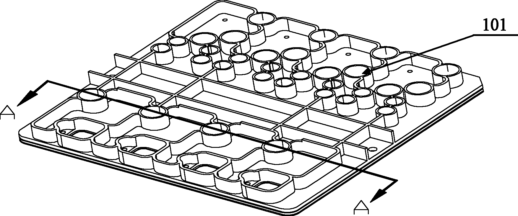
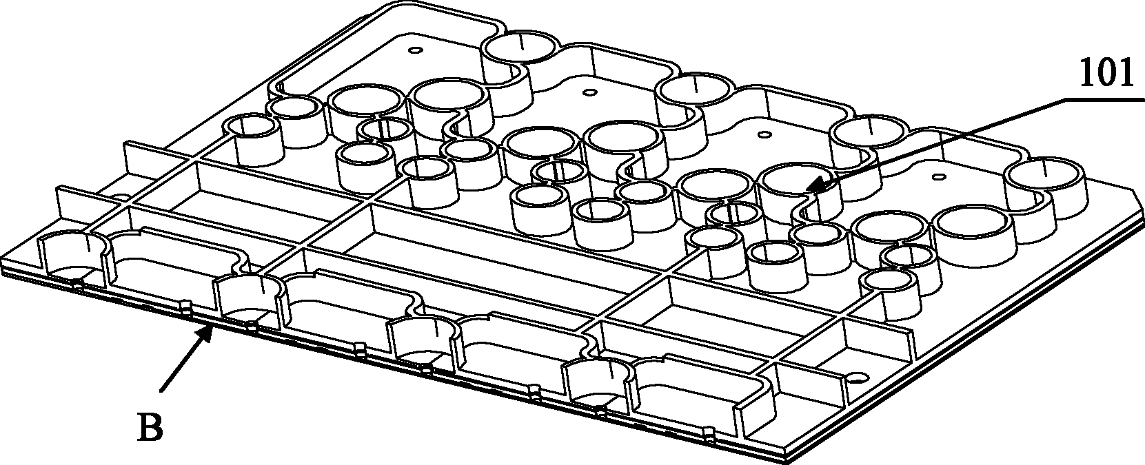
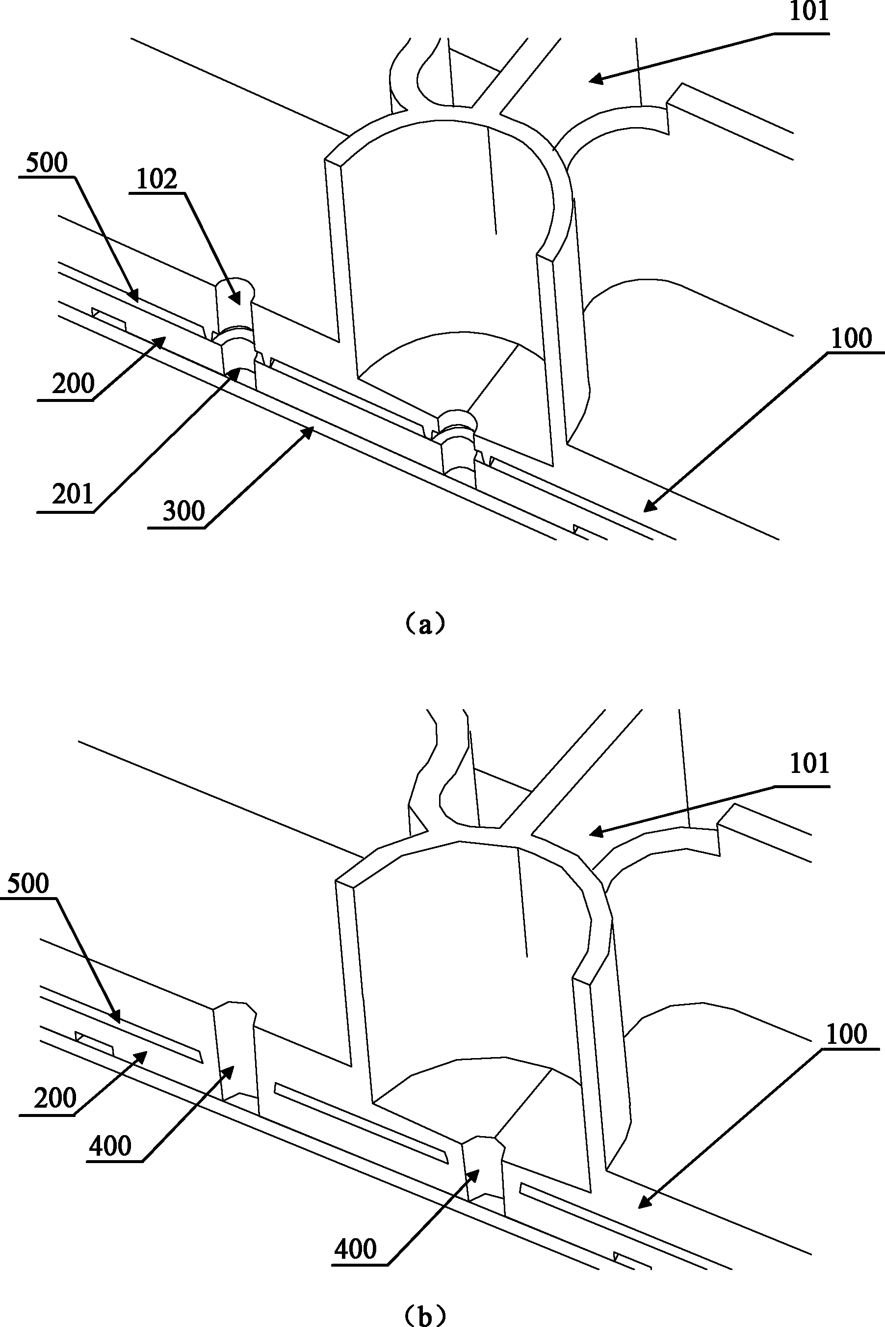
[0047] Such as figure 1 , figure 2 , image 3 As shown in (a) and (b), the overall structure of the membrane movable polymer microfluidic chip of this embodiment includes: a first substrate 100, a diaphragm 300, and several structural components 101 on one side of the first substrate 100 , A number of first through holes 102 on the first substrate 100. The structural components 101 are various channels, containers, and external mechanisms in the chip. The chip also includes a second substrate 200, one side of the second substrate 200 is attached to the other side of the first substrate 100. In order to facilitate the sticking of the diaphragm and prevent defects or bubbles in the sticking area after sticking, the other surface of the second substrate 200 is a flat surface. The second substrate 200 is provided with a second through hole 201 corresponding to the first through hole 102 of the first substrate 100. The first through hole 102 and the second through hole 201 form an...

Embodiment 2

[0051] This embodiment provides a method for manufacturing the membrane movable polymer microfluidic chip in embodiment 1, which includes the steps of preparing a first substrate 100 and a second substrate 200, and the surface of the first substrate facing away from the structural component is a welding surface, The surface of the second substrate 200 that is attached to the first substrate 100 is a soldering surface, and at least one fuse is provided on the soldering surface of the first substrate 100 or the second substrate 200; the first substrate 100 and the second substrate 200 are attached The welding surface of the fusion line is melted to weld the first substrate 100 and the second substrate 200 together; after welding, the diaphragm 300 is attached to the surface (non-welded surface) of the second substrate 200.

[0052] Such as Figure 4 As shown, in this embodiment, an ultrasonic indenter is used to melt the fuse to weld the first substrate 100 and the second substrate ...

Embodiment 3

[0058] Such as Image 6 As shown, the preparation method of the membrane movable polymer microfluidic chip of this embodiment is basically the same as the method of embodiment 2, that is, the first substrate 100 and the second substrate 200 are prepared, and the surface of the first substrate facing away from the structural components is the welding surface , The surface of the second substrate 200 that is attached to the first substrate 100 is a welding surface, and at least one fuse is set on the welding surface of the first substrate 100 or the second substrate 200; the first substrate 100 and the second substrate are attached The welding surface of 200 is melted to weld the first substrate 100 and the second substrate 200 together; after welding, the diaphragm 300 is attached to the surface (non-welded surface) of the second substrate 200.

[0059] The difference is that a laser is used to melt the fuse to weld the first substrate 100 and the second substrate 200. Therefore, ...


PUM


Abstract

A membrane mobile polymer microfluidic chip and a preparation method of the same. The microfluidic chip comprises: a first substrate (100), a membrane (300), several structure parts (101) located on one surface of the first substrate (100), several first through holes (102) located on the first substrate (100), and a second substrate (200). One surface of the second substrate (200) is attached to the other surface of the first substrate (100), and the other surface of the second substrate (200) is smooth. The second substrate (200) is provided with a second through hole (201) corresponding to the first through hole (102) of the first substrate (100). The first through hole (102) and the second through hole (201) form an integral through hole (400). The membrane (300) is attached to the other surface of the second substrate (200). The preparation method comprises the following steps: disposing at least one fuse wire (103, 202) on welding surfaces of a first substrate (100) and a second substrate (200); and attaching the first substrate (100) to the second substrate (200) and fusing the fuse wire (103, 202) to welding the first substrate (100) to the second substrate (200), and after welding, attaching a membrane (300) to a surface of the second substrate (200).

Description

Technical field [0001] The invention relates to the technical field of manufacturing a membrane-moving polymer microfluidic chip, in particular to a membrane-moving polymer microfluidic chip and a preparation method thereof. Background technique [0002] Microfluidics is the use of technology to manipulate micro-volume fluids, applied to the structure and control methods of biological and chemical fluid systems. The applications and potential applications of microfluidics include disease diagnosis, life science research, and biological and / or chemical sensor development. [0003] The membrane-moving polymer microfluidic structure includes a substrate, which has one or more microfluidic channels or paths, and a cover plate or a second or more sub-substrate, which has fluid paths that may or may not be interconnected. These microfluidic structures can be collectively referred to as microfluidic chips. [0004] Microfluidic chips can be made of glass, quartz or silicon. These chips ty...

Claims


Application Information

Patent Timeline
Patent Type & Authority Patents(China)
IPC IPC(8): B01L3/00B23K26/20B23K26/42B29C65/16
CPCB29C65/08B01L2300/0816B81C1/00119B29C66/30223B29C65/1635B29C65/7844B23K26/20B81C2203/035B29C65/16B01L2200/027B29C66/3242B81B2201/058B23K26/42B81B2203/0127B29C66/54B23K11/02B01L2200/0689B23K2201/18B23K11/002B23K26/246B23K26/3246B01L3/502707B01L3/00B29L2031/756B29C65/1696B81C3/001B23K26/244B23K26/324B23K2101/18B23K2103/30B29C66/8322
Inventor 杨奇
Owner BEIJING BOHUI INNOVATION TECH
Why Eureka
Try Eureka