Preparation method for solar wafer

A technology for solar wafers and wafers, which is applied in the manufacturing of final products, sustainable manufacturing/processing, electrical components, etc., can solve the problems of inability to precisely control the concentration of doping ions, complicated thermal diffusion process steps, and bending of silicon wafers. The effect of mixing uniformity, reducing compounding effect and reducing bending

Inactive Publication Date: 2012-02-01
KINGSTONE SEMICONDUCTOR LIMITED COMPANY
View PDF7 Cites 3 Cited by
  • Summary
  • Abstract
  • Description
  • Claims
  • Application Information

AI Technical Summary

Problems solved by technology

[0012] The technical problem to be solved by the present invention is to overcome the defects that the concentration of dopant ions cannot be accurately controlled, the steps of the thermal diffusion process are complicated, and the silicon wafer is bent due to uneven stress in the thermal diffusion process of the prior art. A method for preparing solar wafers that can precisely control the concentration of doping ions and eliminate the stress field at the junction of aluminum and silicon

Method used


Image

  • Preparation method for solar wafer
  • Preparation method for solar wafer
  • Preparation method for solar wafer

Examples


Embodiment Construction

[0035] The preferred embodiments of the present invention are given below in conjunction with the accompanying drawings to describe the technical solution of the present invention in detail.

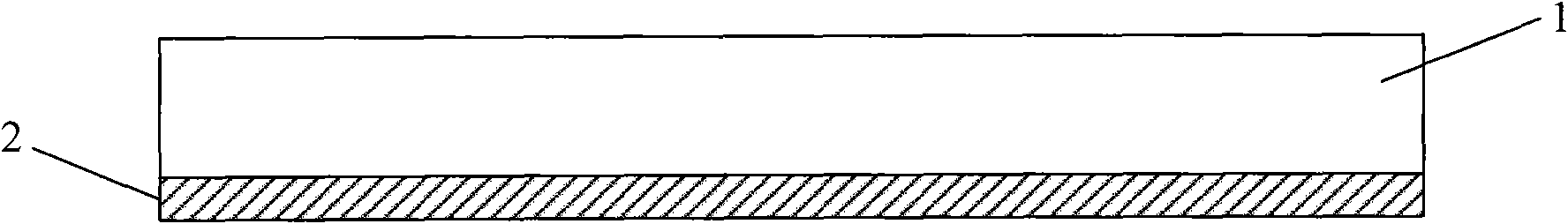
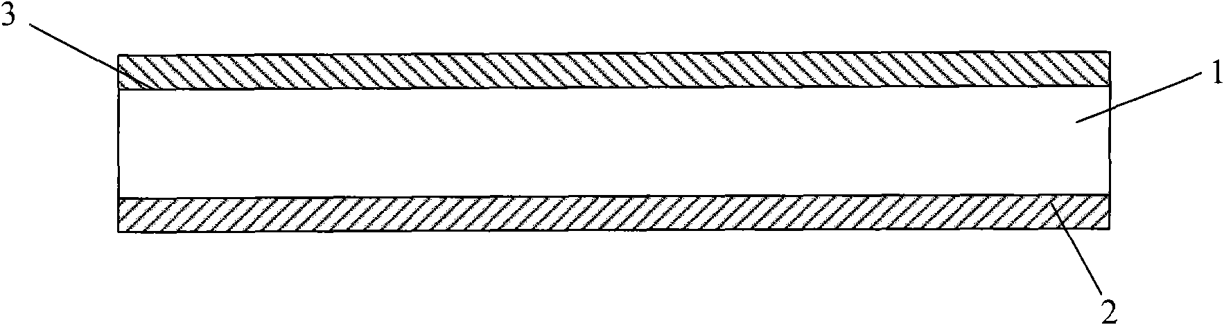
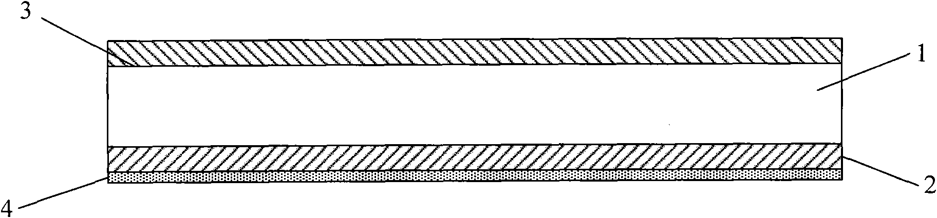
[0036] refer to Figure 1-Figure 6 , introduce in detail the preparation method of the solar wafer of the present invention, especially relate to the preparation method of the backside field of the solar cell, take the solar wafer of P-type substrate 1 as an example, introduce the preparation method of the solar wafer of the present invention, especially for the solar cell The fabrication method of the selective emitter comprises the following steps:

[0037] refer to figure 1 , step S 1 , implanting P-type ions such as boron ions by ion implantation on the back of the wafer based on P-type semiconductors to form a P+-type doped layer 2, the doped P-type ions are accelerated to 10-50keV, doped Concentration can be 2E15-7E15 / cm 3 Of course, those skilled in the art can also select ot...


PUM


Abstract

The invention discloses a preparation method for a solar wafer, which comprises the following steps of: S1) implanting P-type ions into the backside of a P-type substrate wafer through an ion implantation method to form a P+ doped layer; S2) forming an N-type doped layer on the surface of the P-type substrate wafer; S3) plating a silicon nitride film on the surface of the P-type substrate wafer; S4) making a metal electrode on the surface of the P-type substrate wafer and sintering to form a surface electrode; and S5) making a metal electrode on the backside of the P-type substrate wafer and sintering to form a backside electrode, wherein when a P type is replaced by an N type, the N type is replaced by the P type at the same time. By adopting the ion implantation method, the doped layers can be enabled to be even, the doping dose can be accurately controlled and therefore the conversion efficiency of a solar cell can be enabled to be closer to a theoretic design value.

Description

technical field [0001] The invention relates to a method for preparing a solar wafer, in particular to a method for preparing a solar wafer in the back field of a solar cell by means of ion implantation. Background technique [0002] New energy is one of the five most decisive technological fields in the world economic development in the 21st century. Solar energy is a clean, efficient and inexhaustible energy source. In the new century, the governments of various countries regard the utilization of solar energy resources as an important content of the national sustainable development strategy. Photovoltaic power generation has the advantages of safety, reliability, no noise, no pollution, less constraints, low failure rate, and easy maintenance. In recent years, with the rapid development of photovoltaic power generation in the world, the supply of solar chips is in short supply, so improving the photoelectric conversion efficiency of solar chips and the production capaci...

Claims


Application Information

Patent Timeline
Patent Type & Authority Applications(China)
IPC IPC(8): H01L31/18
CPCY02P70/50
Inventor 陈炯
Owner KINGSTONE SEMICONDUCTOR LIMITED COMPANY
Why Eureka
Try Eureka