
Voltage buffer applied to high-speed analogue-to-digital converter

A voltage buffer, analog-to-digital converter technology, applied in the direction of analog-to-digital converter, physical parameter compensation/prevention, etc., can solve problems such as limiting reference voltage speed and large time constant

Active Publication Date: 2012-02-15
TSINGHUA UNIV
View PDF3 Cites 8 Cited by
  • Summary
  • Abstract
  • Description
  • Claims
  • Application Information

AI Technical Summary

Problems solved by technology

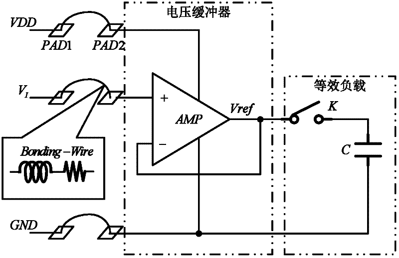
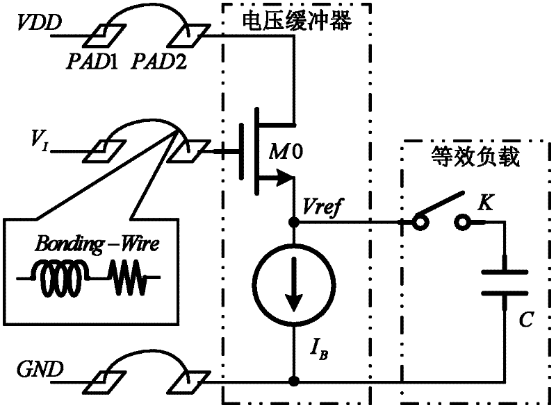
The outstanding problem of this structure is that its output resistance is at 1 / g m0 magnitude (g m0 It is the transconductance of the M0 tube, which is used to describe the ability of the MOS tube to convert voltage into current. For details, please refer to related analog circuit books, such as "Design of Analog CMOS Integrated Circuits", Behzad Razavi), the time constant determined by the resistance is still Larger, which limits how quickly the reference voltage can reach the rated accuracy

Method used


Image

  • Voltage buffer applied to high-speed analogue-to-digital converter
  • Voltage buffer applied to high-speed analogue-to-digital converter
  • Voltage buffer applied to high-speed analogue-to-digital converter

Examples


Embodiment Construction

[0017] The voltage buffer suitable for high-speed analog-to-digital converter proposed by the present invention is described in detail as follows in conjunction with the accompanying drawings and embodiments:

[0018] The embodiment of the voltage buffer suitable for high-speed analog-to-digital converter proposed by the present invention is as follows Figure 4 indicated by the dotted box. It includes three PMOS transistors M3, M2 and M4; three NMOS transistors M1, M5 and M6; except for the power supply VDD and ground GND, the positive reference input voltage is V IP , the positive reference output voltage is VRP, and the negative reference input voltage is V IN , the negative reference output voltage is VRN. The positive end load is equivalent to capacitor C1 and switch K1, and the negative end load is equivalent to capacitor C2 and switch K2; in the figure, PAD1 is the substrate solder joint; PAD2 is the chip solder joint; the bonding-wire between PAD1 and PAD2 is Metal ...


PUM


Abstract

The invention relates to a voltage buffer applied to a high-speed analogue-to-digital converter, and belongs to the field of mixed signal integrated circuit designing. The voltage buffer comprises three P-channel metal oxide semiconductor (PMOS) transistor and three N-channel metal oxide semiconductor (NMOS) transistors. Connection relationships among the MOS transistors are that: the drain and gate of a first NMOS transistor are connected together and connected to the gate of the second PMOS transistor and the drain of the first PMOS transistor; a positive reference input voltage is connected to the gate of the first PMOS transistor after passing through a bonding wire; the source of the first PMOS transistor and the drain of the second PMOS transistor are connected together; the sources of the second and third PMOS transistors are connected together and finally connected to an external power potential after passing through the bonding wire; the drain and gate of the third PMOS transistor are connected together and connected to the gate of the third NMOS transistor and the drain of the second NMOS transistor; a negative reference input voltage is connected to the gate of the second NMOS transistor after passing through the bonding wire; the source of the second NMOS transistor and the drain of the third NMOS transistor are connected together; and the sources of the first and third NMOS transistors are connected together and finally connected to an external ground potential after passing through the bonding wire. The voltage buffer has the characteristics of higher charging speed and reference voltage capable of reaching rated accuracy faster.

Description

technical field [0001] The invention belongs to the field of mixed-signal integrated circuit design, in particular to a voltage buffer, which can quickly stabilize the on-chip reference voltage. Background technique [0002] Currently the most common chip packaging method is COB (Chip On Board), and COB can be connected by wire bonding or flip-chip connection. [0003] Wire bonding, as the name suggests, fixes the chip on the circuit substrate, and connects the pins of the chip to the corresponding points on the substrate with the help of thin metal bonding wires. Wire bonding is the most mature way at present, but as As the working speed of the chip increases, the role of the inductance introduced by the thin metal bonding wire begins to emerge. The inductance of the bonding wire causes the internal oscillation of the chip, etc., which greatly restricts the improvement of the working speed of the chip. The flip-chip connection uses a special process to generate correspondi...

Claims


Application Information

Patent Timeline
IPC IPC(8): H03M1/06H03M1/12
Inventor 周礼兵刘力源李冬梅
Owner TSINGHUA UNIV
Learn More