Preparation method of conductive polymer one-dimensional nanostructured array

A technology of conductive polymers and nanostructures, applied in the field of polymer materials, to achieve rapid migration, improved device performance, and easy operation

Inactive Publication Date: 2012-02-22
UNIV OF ELECTRONICS SCI & TECH OF CHINA
View PDF7 Cites 12 Cited by
  • Summary
  • Abstract
  • Description
  • Claims
  • Application Information

AI Technical Summary

Problems solved by technology

[0007] Judging from the current research, the research on PEDOT ordered nano-films has made some progress, but there are still many problems, the most important of which is the stable and reliable assembly of ordered nano-structures, which is very important for the device after the device is prepared. Performance has a very heavy impact

Method used


Image

  • Preparation method of conductive polymer one-dimensional nanostructured array
  • Preparation method of conductive polymer one-dimensional nanostructured array

Examples


Embodiment 1

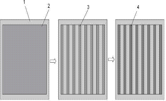
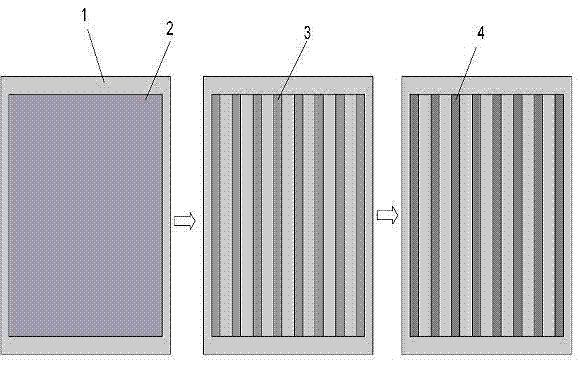
[0041] Dissolve a certain proportion of the oxidant material in the chloroform solution and stir it evenly, then use a dropper to suck a small amount of oxidant / chloroform solution and slowly drop it on the substrate placed on the spin coater, and control the spin coater's speed to prevent too much speed Film cannot be formed too slowly or the film is not dense enough. After the oxidant film with a certain thickness and uniformity is obtained, the substrate on which the oxidant film is deposited is placed in a vacuum oven for drying for a certain period of time to cure the film and drive out the chloroform solvent. To obtain an oxidant spin-coated film, such as figure 1 Shown in 2.

[0042] in figure 1 In, the oxidant spin-coated film obtained in 2 is subjected to an electron beam etching method to obtain an oxidant one-dimensional nanostructure array.

[0043] in figure 1 Then, the one-dimensional nanostructure array of the oxidant is further exposed to the atmosphere of the cond...

Embodiment 2

[0051] The monomer material is pyrrole.

[0052] The preparation process of the one-dimensional nanostructure array is similar to that of the first embodiment. Since the monomer material is pyrrole, a polypyrrole one-dimensional nanostructure array is obtained.

[0053] The etching line width is 150 nanometers, thereby obtaining a polypyrrole one-dimensional nanostructure array with a width of 150 nanometers.

Embodiment 3

[0055] The monomer material is pyrrole.

[0056] The preparation process of the one-dimensional nanostructure array is similar to that of the first embodiment. Since the monomer material is pyrrole, a polypyrrole one-dimensional nanostructure array is obtained.

[0057] The etching line width is 120 nanometers, thereby obtaining a polypyrrole one-dimensional nanostructure array with a width of 120 nanometers.


PUM

PropertyMeasurementUnit
widthaaaaaaaaaa
widthaaaaaaaaaa

Abstract

The invention discloses a preparation method of a conductive polymer one-dimensional nanostructured array. First, an oxidizing agent film is prepared by a spin coating method; then, an oxidizing agent one-dimensional nanostructured array is prepared by an etching method; and finally, the oxidizing agent one-dimensional nanostructured array is exposed to a conductive polymer monomer atmosphere and initiated for polymerization through an in-situ chemical polymerization, so as to obtain the conductive polymer one-dimensional nanostructured array. The preparation method of the polymer nanostructured array provided by the invention overcomes defects in a prior art, and is reasonable, simple and easy for operation.

Description

technical field [0001] The invention relates to the field of polymer materials, in particular to a method for preparing a conductive polymer ordered micro / nano structure array. Background technique [0002] In recent years, conductive polymer materials with regular morphology (such as balls, wires, ribbons, tubes, etc.) in the micro- and nano-scale range have become a research hotspot for scientists from all over the world. After these novel conductive polymer nanostructures interact with certain media in the atmosphere, due to the large specific surface area and excellent surface conditions of the material, the gas molecules can be adsorbed / desorbed on the surface of the sensitive material quickly, making the gas sensor With the characteristics of fast response, high selectivity, and room temperature operation, it is a research hotspot for the next generation of gas sensor sensitive materials. However, at present, this conductive polymer material is basically in a disorder...

Claims


Application Information

Patent Timeline
Patent Type & Authority Applications(China)
IPC IPC(8): B81C1/00C08G61/12C08G73/06
Inventor 杨亚杰蒋亚东徐建华
Owner UNIV OF ELECTRONICS SCI & TECH OF CHINA
Why Eureka
Try Eureka