Epitaxy production method of light emitting diode (LED)

A technology for light-emitting diodes and production methods, which is applied to electrical components, circuits, semiconductor devices, etc., can solve the problems of poor current expansion capability and small internal capacitance of GaN-based LEDs, and achieves improved antistatic capability, improved luminous efficiency, and increased luminous efficiency. The effect of productivity

Inactive Publication Date: 2012-02-29
YANGZHOU ZHONGKE SEMICON LIGHTING
View PDF4 Cites 19 Cited by
  • Summary
  • Abstract
  • Description
  • Claims
  • Application Information

AI Technical Summary

Problems solved by technology

[0009] The present invention solves the problems of small internal capacitance and poor current expansion capability of GaN-based LEDs by inserting a modulated doped nGaN/uGaN periodic structure between nGaN and the light-emitting layer, so as to increase the internal capacita

Method used


Image

  • Epitaxy production method of light emitting diode (LED)
  • Epitaxy production method of light emitting diode (LED)
  • Epitaxy production method of light emitting diode (LED)

Examples


Embodiment Construction

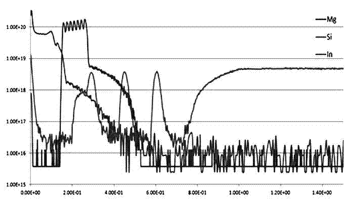
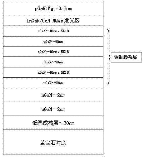
[0022] 1. Principles of the epitaxial processing steps of light-emitting diodes:

[0023] 1. The low-temperature gallium nitride nucleation layer grown on sapphire, silicon carbide, silicon, gallium arsenide, zinc oxide or lithium aluminate substrate, the growth temperature is 500-600 ℃, the growth pressure is 10000-90000Pa, the growth thickness 0.01-0.1 μm.

[0024] 2. Growing an unintentionally doped GaN layer on the low-temperature gallium nitride nucleation layer, the growth temperature is 900-1200°C, the growth pressure is 10000-60000Pa, and the growth thickness is 1-5μm.

[0025] 3. N-type doped GaN is grown on the unintentionally doped GaN layer, the growth temperature is 1000-1100°C, the growth pressure is 10000-60000Pa, the growth thickness is 1-5μm, and the N-type doping element is Si or Other elements that can act as N-type impurities in GaN.

[0026] 4. Grow N-type doped GaN and non-doped GaN alternating periodic structure layers on N-type doped GaN, the growth t...


PUM

PropertyMeasurementUnit
Growth temperatureaaaaaaaaaa
Growth pressureaaaaaaaaaa
Growth thicknessaaaaaaaaaa

Abstract

An epitaxy production method of a light emitting diode (LED) relates to a semiconductor technology field. A low temperature aluminum nitride gallium indium nucleating layer, an unintended doped gallium nitride layer, a doping gallium nitride layer, a doped GaN and non-doped GaN alternative periodic structure layer, an InGaN /GaN of multiple quantum well luminescence layer and a doped gallium nitride layer are successively grown on a substrate. In the invention, the doped GaN and non-doped GaN alternative growing periodic structure is inserted between the doping GaN and a multiple quantum well luminescence region so that internal capacitance of a GaN-based LED device can be increased and a current expansion ability of the GaN-based LED can be improved. Therefore, antistatic performance can be improved; a working voltage of the GaN-based LED can be reduced and a luminous efficiency can be raised.

Description

technical field [0001] The invention belongs to the technical field of semiconductor production, in particular to the epitaxial structure design and growth method of gallium nitride-based light-emitting diodes. Background technique [0002] The current semiconductor lighting technology based on gallium nitride-based light-emitting diodes (LEDs) is penetrating into all aspects of social life, such as landscape lighting, special lighting, and liquid crystal backlight lighting. However, due to the inherent defects, high dislocation density, and poor material quality of III-nitrides, semiconductor lighting devices based on III-nitrides have poor antistatic ability, and the current expansion capability of traditional positive-mounted LED devices is poor. Two aspects greatly limit its further entry into the high-end application market. [0003] For example, adding Zener diodes during packaging, electrostatic rings during operation, etc., and adding various insertion layers into t...

Claims


Application Information

Patent Timeline
IPC IPC(8): H01L33/00
Inventor 李志聪李鸿渐李盼盼李璟王国宏
Owner YANGZHOU ZHONGKE SEMICON LIGHTING
Why Eureka
Try Eureka