Semiconductor device and manufacturing method thereof

A manufacturing method and semiconductor technology, applied in semiconductor/solid-state device manufacturing, semiconductor devices, semiconductor/solid-state device components, etc., can solve problems such as device performance degradation, high contact plug resistance, reliability problems, etc., to reduce parasitic Effects of resistance, performance improvement, and high conductivity

Active Publication Date: 2012-03-14
锐立平芯微电子(广州)有限责任公司
View PDF4 Cites 6 Cited by
  • Summary
  • Abstract
  • Description
  • Claims
  • Application Information

AI Technical Summary

Problems solved by technology

Although the Cu contact technology solves the problem of high contact plug resistance, on the other hand,

Method used


Image

  • Semiconductor device and manufacturing method thereof
  • Semiconductor device and manufacturing method thereof
  • Semiconductor device and manufacturing method thereof

Examples


no. 1 example

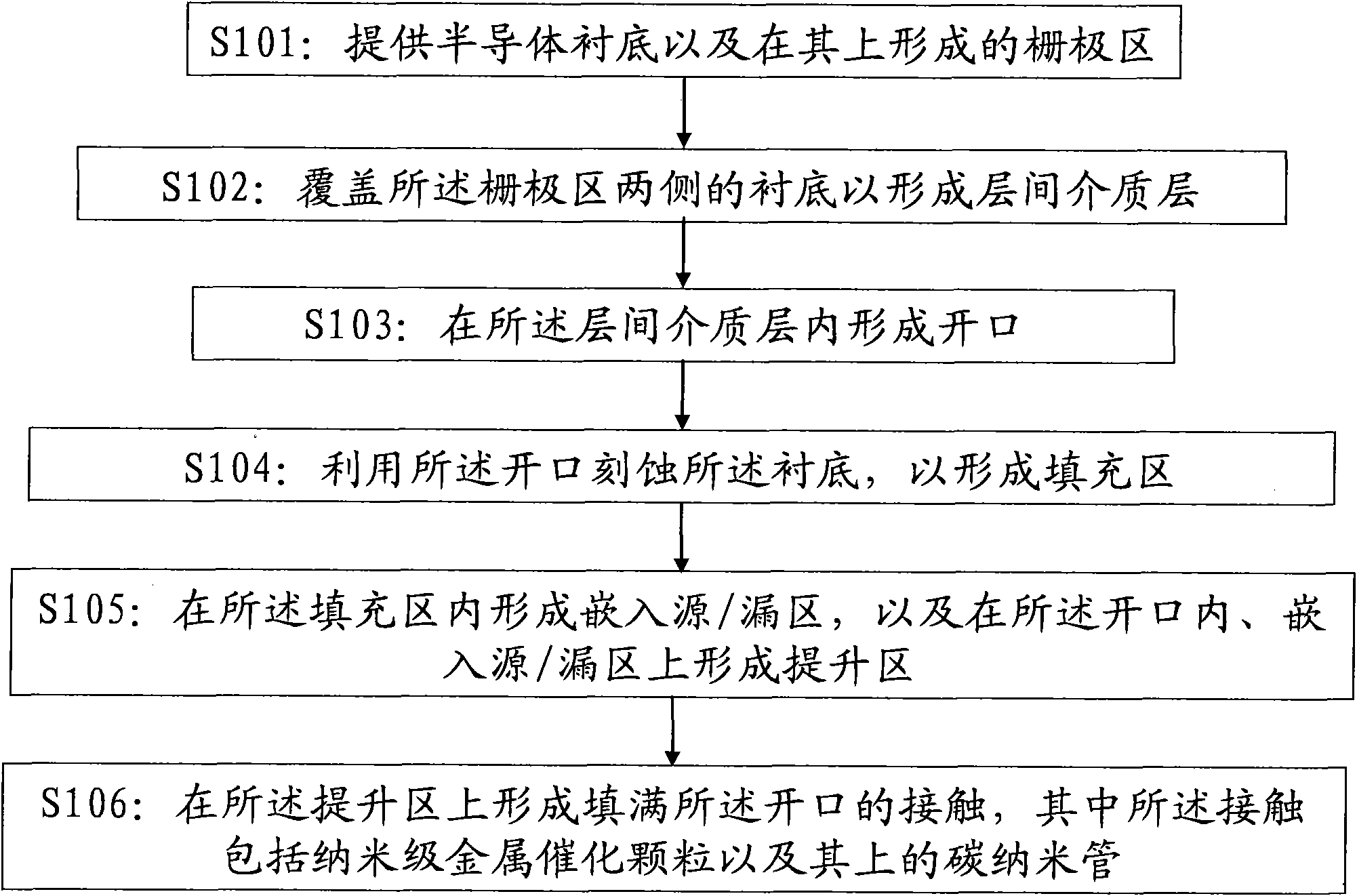
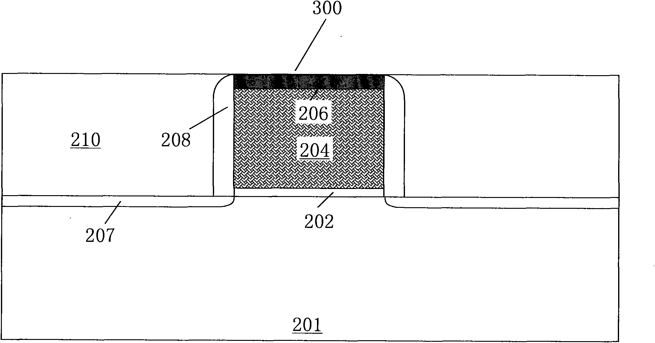
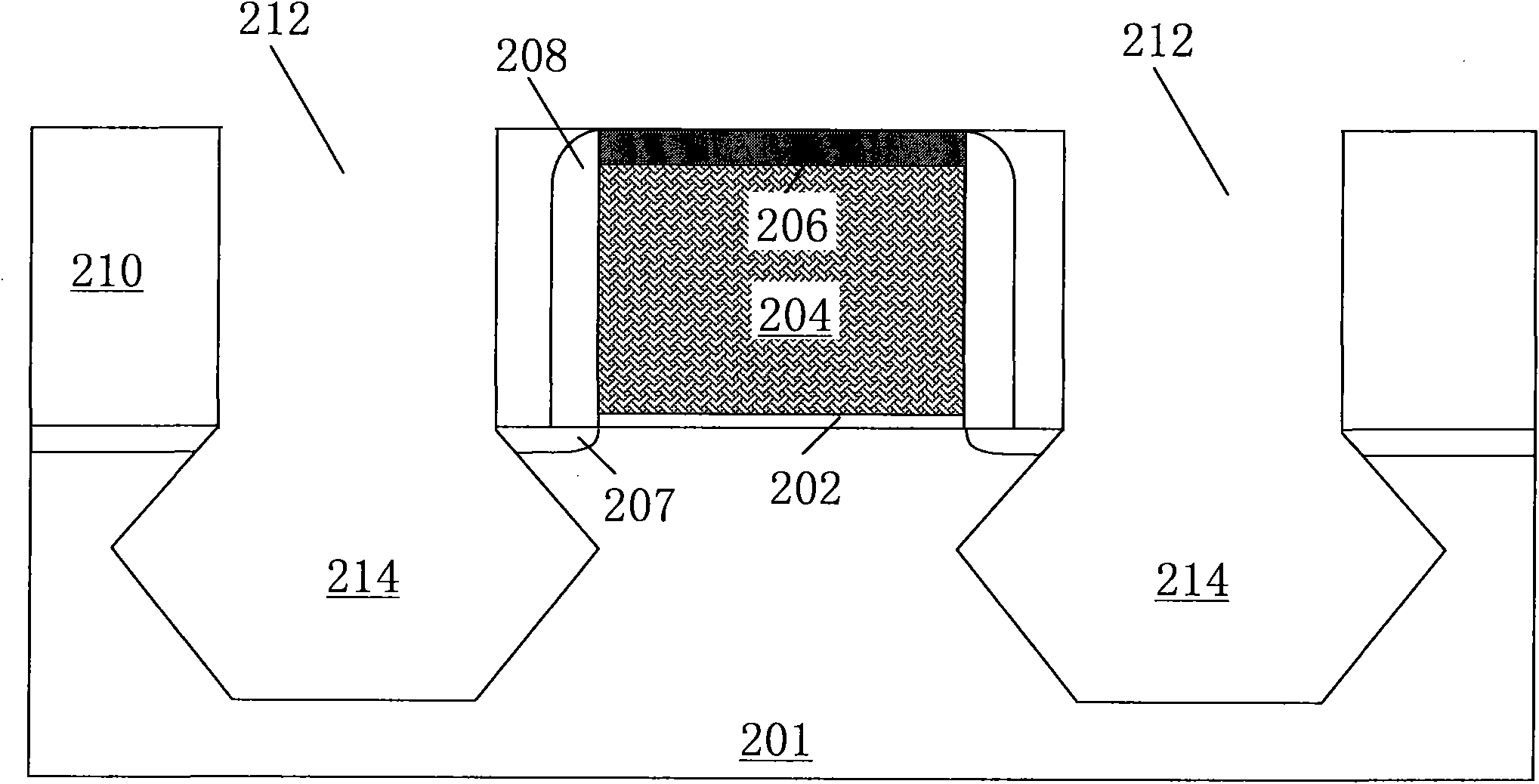
[0015] refer to figure 1 , figure 1 A flowchart of a method for manufacturing a semiconductor device according to a first embodiment of the present invention is shown. In step S101, a semiconductor substrate 201 and a gate region 300 formed thereon are provided, refer to figure 2 . In this embodiment, the substrate 201 has been pre-processed, and the processing operations include pre-cleaning, forming a well region and forming a shallow trench isolation region. In this embodiment, the substrate 201 is silicon The substrate. In other embodiments, the substrate 201 may also include other compound semiconductors, such as silicon carbide, gallium arsenide, indium arsenide or indium phosphide. The substrate 201 may include various doping configurations according to design requirements known in the art (eg, p-type substrate or n-type substrate). In addition, preferably, the substrate 201 includes an epitaxial layer, and the substrate 201 may also include a silicon-on-insulator ...

no. 2 example

[0023] Only the aspects of the second embodiment that differs from the first embodiment will be described below. Parts not described should be considered to be performed using the same steps, methods or processes as those in the first embodiment, so details will not be repeated here.

[0024] refer to Figure 10 , Figure 10 A flowchart of a method for manufacturing a semiconductor device according to a second embodiment of the present invention is shown. In step S201, a semiconductor substrate 201 and a gate region 300 formed thereon are provided, and source / drain doped regions 216 are formed in the substrate on both sides of the gate region, refer to Figure 11 . The substrate 201 and the gate region 300 are the same as those in the first embodiment, and will not be repeated here. The source / drain doped region 216 can be formed by implanting p-type or n-type dopants or impurities into the substrate 200 according to the desired transistor structure, which can be formed by...


PUM


Abstract

The invention discloses a semiconductor device and a manufacturing method thereof. According to the invention, after source/drain regions or lifting regions are formed, a contact plug structure containing nano-scale catalytic metal particles and carbon nanotubes on the nano-scale catalytic metal particles is formed. The nano-scale catalytic metal particles not only has an effect of inducting growth of the carbon nanotubes but also is capable of reducing contact resistances between contact plug and the source/drain regions in contact holes, so that contact resistances of the device can be reduced; moreover, the carbon nanotubes itself has high conductivity, thereby substantially reducing body resistance for contact; and thus, a parasitic resistance of the device is reduced.

Description

technical field [0001] The present invention generally relates to a semiconductor device and a manufacturing method thereof, in particular to a semiconductor device having a contact plug with low parasitic resistance and a manufacturing method thereof. Background technique [0002] With the rapid development of semiconductor technology, the application of key core technologies of 22nm and below technology MOS process integrated circuits is an inevitable trend in the development of integrated circuits, and it is also one of the topics that major international semiconductor companies and research organizations are competing to develop. At present, the research on source / drain engineering mainly includes: ultra-shallow low-resistance PN junction source / drain technology, low Schottky barrier metal source / drain technology, raised source / drain technology and tungsten (W) / copper ( Cu) mixed contact plug technology, etc. [0003] The traditional contact plug filling material is W, ...

Claims


Application Information

Patent Timeline
IPC IPC(8): H01L21/768H01L23/52
Inventor 王文武赵超王晓磊陈大鹏
Owner 锐立平芯微电子(广州)有限责任公司
Why Eureka
Try Eureka