Parasitic PIN(positive-intrinsic negative) diode in BiCMOS(Bipolar Complementary Metal Oxide Semiconductor) process, and manufacturing method thereof

A PIN diode and process technology, applied in the field of semiconductor integrated circuit manufacturing, can solve the problems of increasing the forward conduction current of the device and increasing the cost, and achieve the effects of improving insertion loss, increasing surface area, and high isolation

Active Publication Date: 2012-03-14
SHANGHAI HUAHONG GRACE SEMICON MFG CORP
View PDF4 Cites 7 Cited by
  • Summary
  • Abstract
  • Description
  • Claims
  • Application Information

AI Technical Summary

Problems solved by technology

Among them, the method of increasing the forward conduction current of the device by adjusting the impurity distribution of the device is very limited.
However, increasing the device area is undoubtedly very unfavorable for the entire circuit. In terms of semiconductor manufacturing costs, increasing the device area also means an increase in cost.

Method used


Image

  • Parasitic PIN(positive-intrinsic negative) diode in BiCMOS(Bipolar Complementary Metal Oxide Semiconductor) process, and manufacturing method thereof
  • Parasitic PIN(positive-intrinsic negative) diode in BiCMOS(Bipolar Complementary Metal Oxide Semiconductor) process, and manufacturing method thereof
  • Parasitic PIN(positive-intrinsic negative) diode in BiCMOS(Bipolar Complementary Metal Oxide Semiconductor) process, and manufacturing method thereof

Examples


Embodiment B

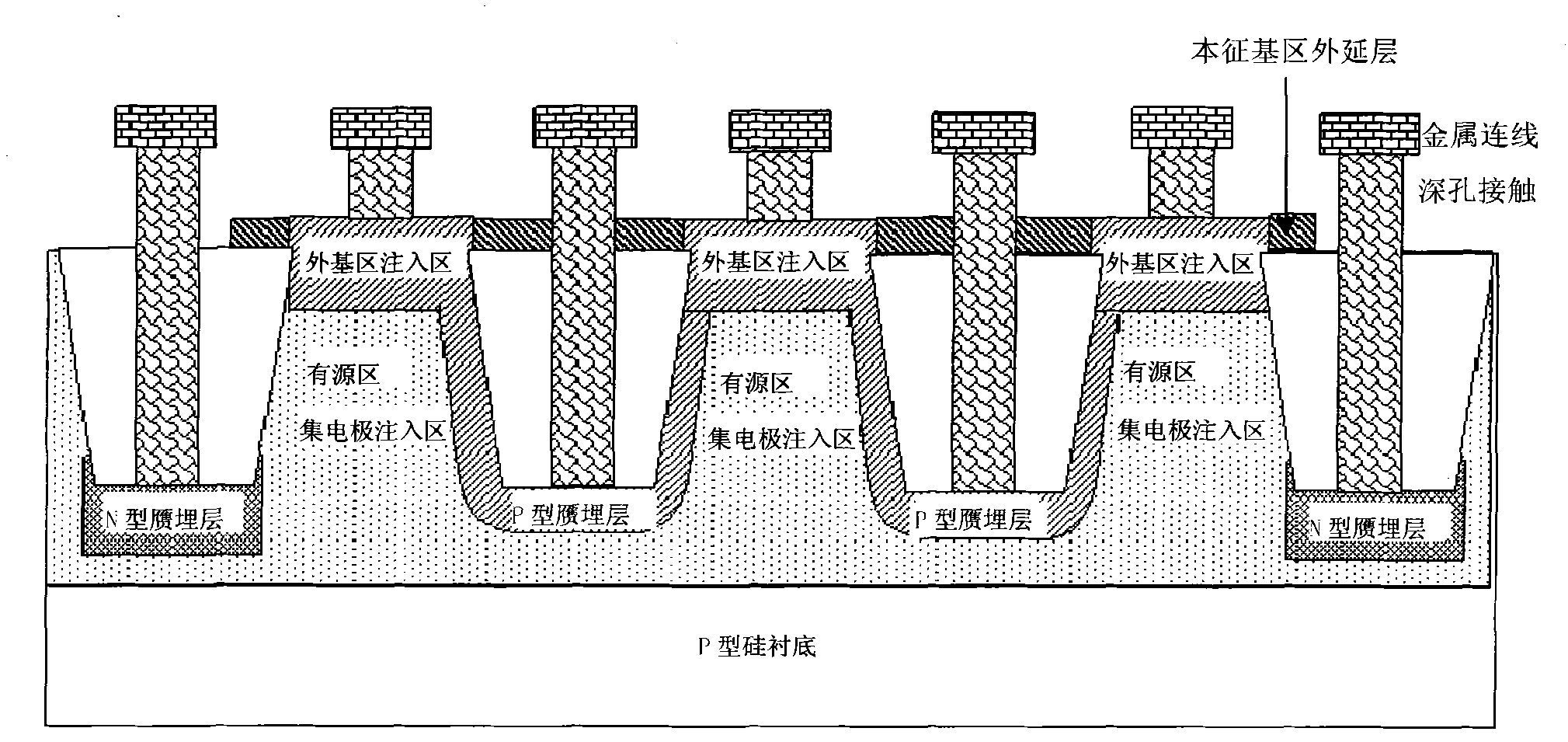
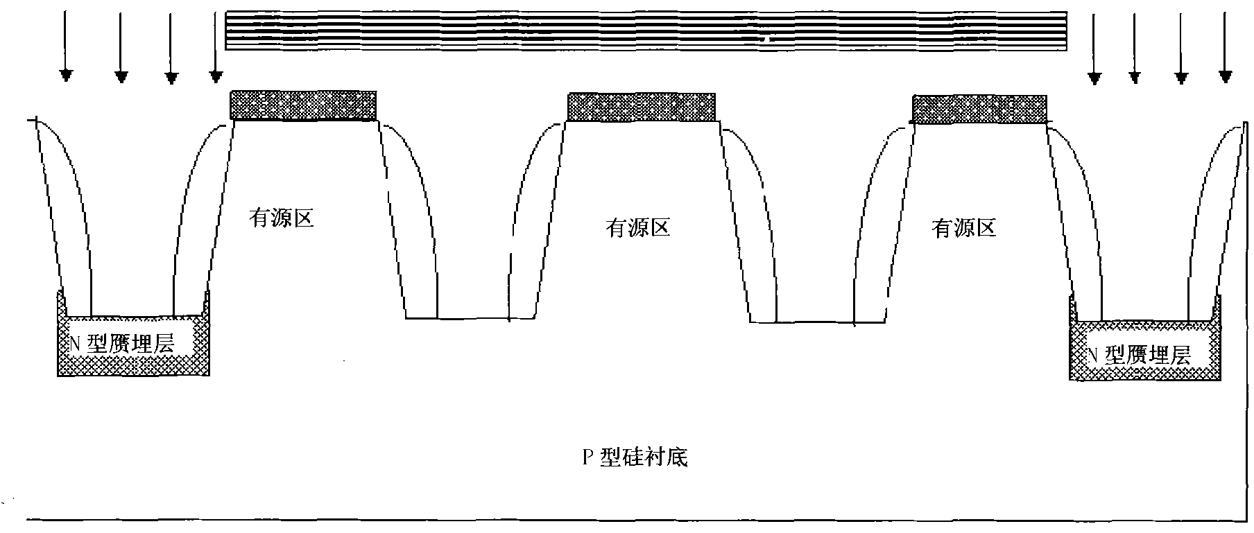
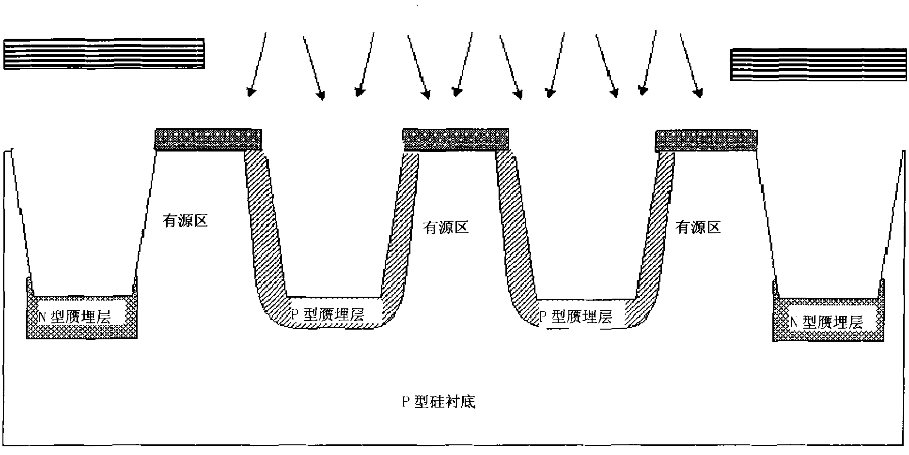
[0022] Such as figure 1 Shown is a device cross-sectional view of a parasitic PIN diode in a BiCMOS process according to an embodiment of the present invention. The parasitic PIN diode in the BiCMOS process of the embodiment of the present invention is formed on a P-type silicon substrate, and the active region is isolated by a shallow trench isolation oxide layer. The parasitic PIN diode includes: an N-type region, an I-type region and a P-type region.

[0023] The I-type region is composed of a plurality of N-type collector implanted regions formed in a plurality of adjacent active regions and connected to each other, and the depth of each of the N-type collector implanted regions is greater than that of the shallow trench isolation oxide layer The bottom of each of the N-type collector injection regions extends into the bottom of the shallow trench isolation oxide layer next to each of the N-type collector injection regions and realizes all the N-type collector injection r...


PUM


Abstract

The invention discloses a parasitic PIN(positive-intrinsic negative) diode in a BiCMOS(Bipolar Complementary Metal Oxide Semiconductor) process, comprising an N type region, an I type region and a P type region, wherein the I type region is composed of multiple N type collector injection regions formed in multiple adjacent active regions; the N type region is composed of an N type buried layer formed at the bottom of a shallow trench isolation oxide layer on the side of the I type region; the P type region is composed of multiple base region epitaxial layers and multiple P type buried layers; the base region epitaxial layers are respectively formed on the top surfaces of the active regions in the I type region; and each P type buried layer is formed on the bottom and side wall of the shallow trench isolation oxide layer in the I type region. The invention also discloses a manufacturing method of the parasitic PIN diode in the BiCMOS process. The invention realizes the aim of providing one more device choice for a circuit without additional process conditions, lower insertion loss and higher isolation are achieved, and the forward on state current of the device is increased and the insertion loss of the device improved while the device area is not increased.

Description

technical field [0001] The invention relates to the field of manufacturing semiconductor integrated circuits, in particular to a parasitic PIN diode in a BiCMOS process; the invention also relates to a method for manufacturing the parasitic PIN diode in a BiCMOS process. Background technique [0002] The bipolar transistor (Bipolar Transistor) in the existing BiCMOS process uses a highly doped buried layer in the collector area to reduce the resistance of the collector area, and uses high-concentration and high-energy N-type implantation to connect the buried layer in the collector area to form a collector Electrode lead-out (collector pick-up). On the buried layer of the collector region, epitaxial low-medium doped collector region, in-situ P-type doped epitaxy forms the base region, and then N-type heavily doped polysilicon constitutes the emitter, and finally completes the production of Bipolar Transistor. Manufacturing parasitic PIN diodes in the existing BiCMOS process...

Claims


Application Information

Patent Timeline
Patent Type & Authority Applications(China)
IPC IPC(8): H01L29/868H01L29/06H01L21/329
Inventor 刘冬华钱文生胡君
Owner SHANGHAI HUAHONG GRACE SEMICON MFG CORP
Why Eureka
Try Eureka