Technology for improving short wave responsibility of semiconductor photoelectric detector

A photodetector and semiconductor technology, applied in the direction of semiconductor devices, circuits, electrical components, etc., can solve the problem that the "dead layer" area cannot be completely eliminated

Inactive Publication Date: 2012-03-14
石郧熙
View PDF1 Cites 2 Cited by
  • Summary
  • Abstract
  • Description
  • Claims
  • Application Information

AI Technical Summary

Problems solved by technology

However, none of these technologies can completely eliminate the existence of the "dead layer" region and the influence of recombination with the semiconductor surface on short-wavelength photogenerated carriers.

Method used


Image

  • Technology for improving short wave responsibility of semiconductor photoelectric detector
  • Technology for improving short wave responsibility of semiconductor photoelectric detector
  • Technology for improving short wave responsibility of semiconductor photoelectric detector

Examples


Embodiment Construction

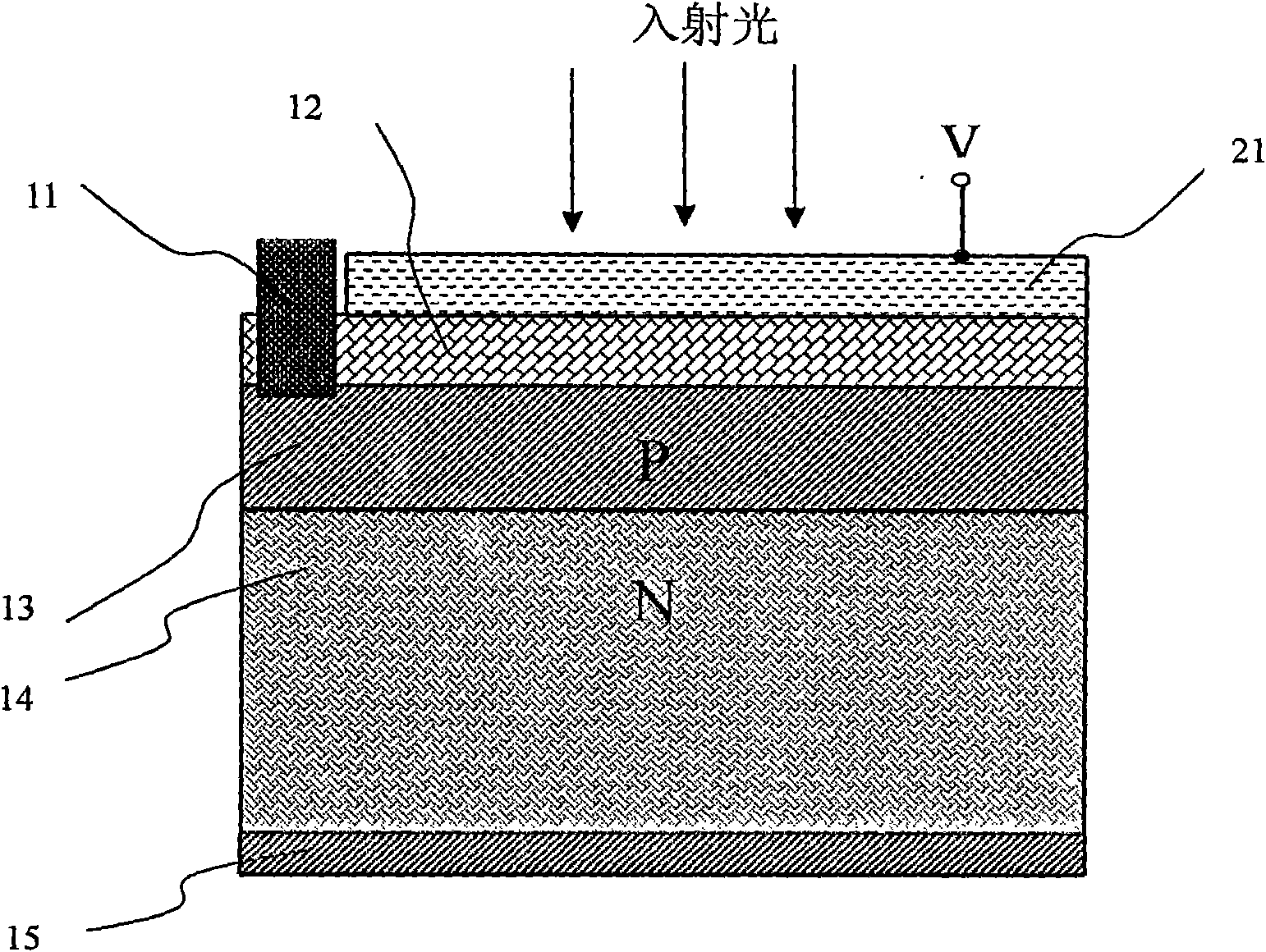
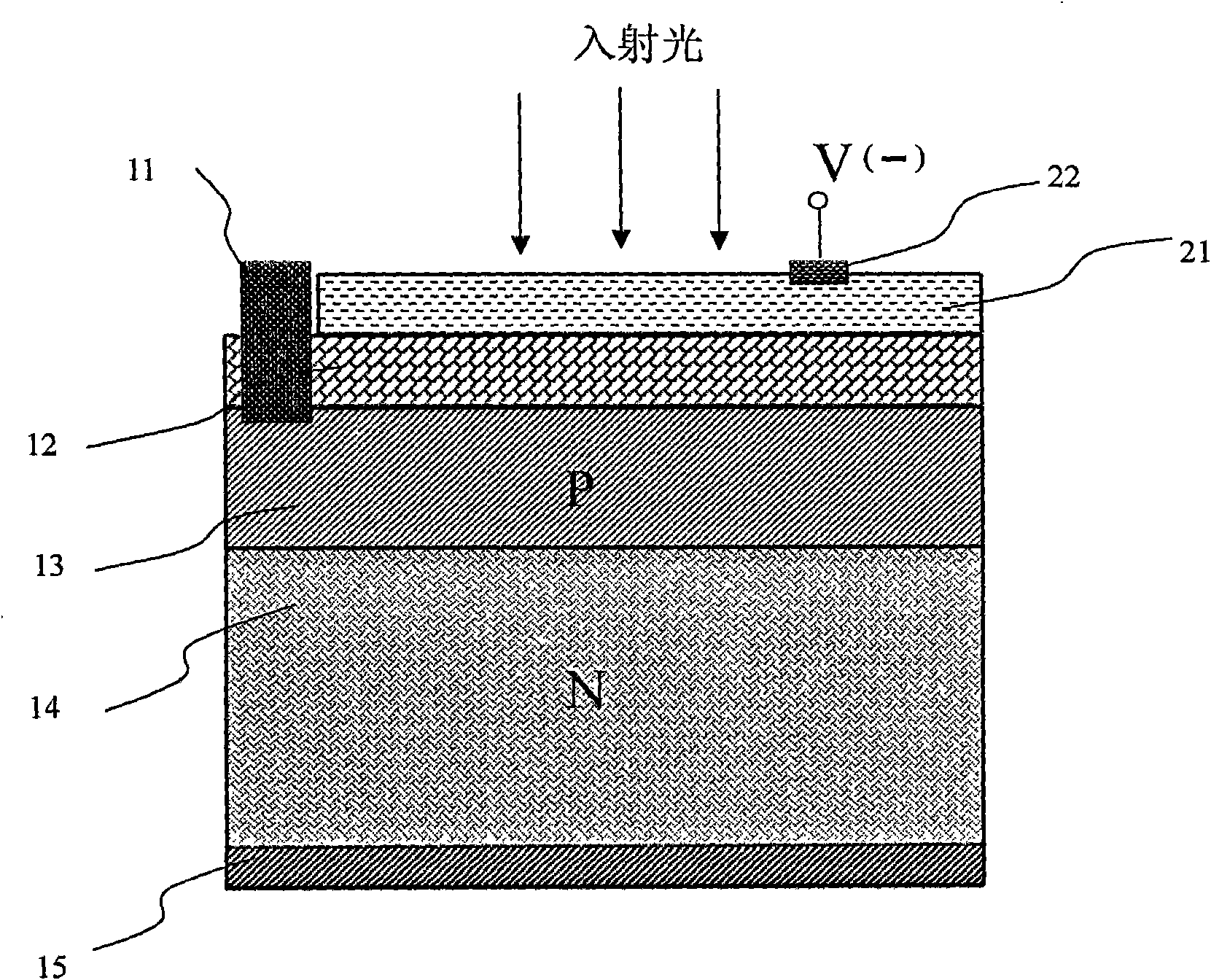
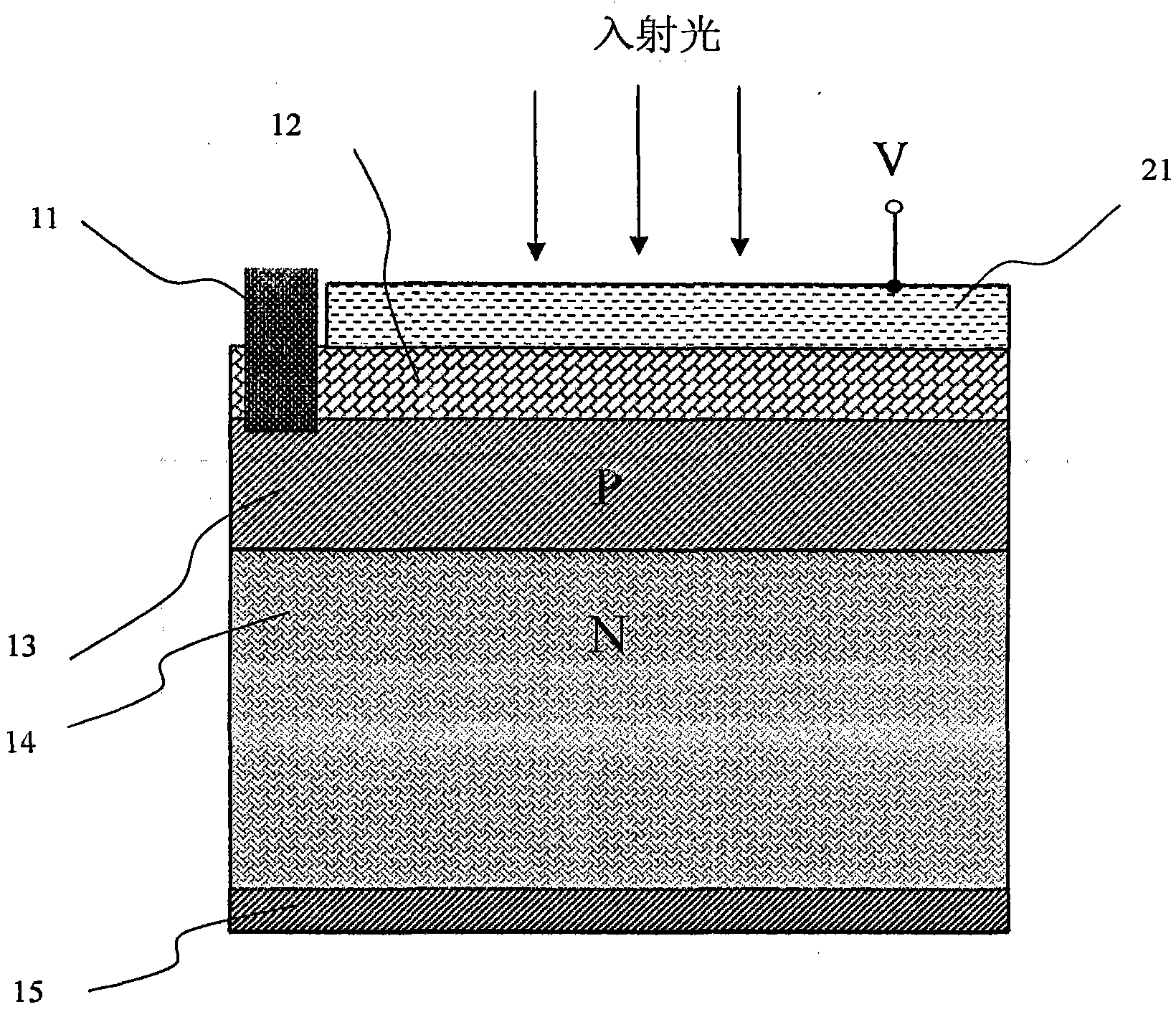
[0012] Attached below figure 2 , a schematic diagram of a p-n junction (p on n) photodetector of Si semiconductor material, specifically illustrating an embodiment of the present invention. The examples are only for illustrating the present invention, and should not be construed as limiting the scope and spirit of the present invention.

[0013] Such as figure 2 :

[0014] Embodiment: 11 and 15 are the output electrodes of p-n junction photodetection of Si semiconductor material, and 12 is dense and pinhole-free SiO 2 Transparent insulating dielectric mask layers, 13 and 14 are p-n junctions of Si semiconductors. SiO 2 The interface between the transparent insulating dielectric mask layer and the underlying semiconductor material is an optical plane. In SiO 2 On the mask layer 12 of the transparent insulating dielectric mask, a transparent conductive thin film layer 21 of indium tin oxide (ITO) and a contact electrode 22 of the transparent conductive thin film layer ar...


PUM


Abstract

The invention belongs to the technical field of a semiconductor photoelectric detector, relating to a technology for improving short wave responsibility of the semiconductor photoelectric detector. The technology comprises the following steps of: adding a transparent conductive thin film layer on the surface of a transparent insulating medium mask layer on the front surface of the semiconductor photoelectric detector, so that a novel structure of the photoelectric detector of a TCOS structure is formed by the transparent conductive thin film layer (TC), the mask layer (O) on the front surface of the detector and the semiconductor (S) below the mask layer; and applying a voltage to the transparent conductive mask layer as a working boost voltage of the semiconductor photoelectric detector to change the surface potential of the semiconductor, a surface energy band and a surface space charge area, reduce the effective surface recombination rate of photo-production minority carriers near the surface of the semiconductor, and remove a 'dead layer' area. Therefore, most of the photo-production minority carriers of the short waves are collected to be a photo-production current, and the short wave responsibility of the semiconductor photoelectric detector is improved. In particular, the technology can be used for effectively improving the short wave responsibility of a high-silicon semiconductor blue-green photoelectric detector or blue-violet photoelectric detector.

Description

Technical field: [0001] The invention belongs to the technical field of semiconductor photodetectors, and relates to a technology for improving the short-wave responsivity of semiconductor photodetectors. A transparent conductive film layer is added on the surface of a transparent insulating medium mask layer on the front surface of a semiconductor photodetector, and the transparent The method of applying a voltage on the conductive film layer as the auxiliary voltage for the semiconductor photodetector to improve the short-wave response of the semiconductor photodetector. In particular, this technology can effectively improve the responsivity of blue-green photodetectors or blue-violet photodetectors in semiconductors such as silicon. Background technique: [0002] In the p-n junction (p on n), p-i-n, APD or CCD silicon semiconductor photodetector made of N-type single crystal silicon or N-type polycrystalline silicon semiconductor material as the substrate, there is a "dea...

Claims


Application Information

Patent Timeline
Patent Type & Authority Applications(China)
IPC IPC(8): H01L31/18
CPCY02P70/50
Inventor 石郧熙
Owner 石郧熙
Why Eureka
Try Eureka