Growth method of germanium substrate and germanium substrate

A growth method and technology of germanium substrate, applied in the direction of single crystal growth, crystal growth, single crystal growth, etc., can solve the problems of poor crystal quality and inability to obtain Ge single crystal layer, etc.

Active Publication Date: 2012-03-21
SHANGHAI SIMGUI TECH +1
View PDF9 Cites 10 Cited by
  • Summary
  • Abstract
  • Description
  • Claims
  • Application Information

AI Technical Summary

Problems solved by technology

However, due to the large lattice mismatch between silicon and germanium, the epitaxial single crystal germanium layer has a large dislocation density and its crystal quality is poor
In

Method used


Image

  • Growth method of germanium substrate and germanium substrate
  • Growth method of germanium substrate and germanium substrate
  • Growth method of germanium substrate and germanium substrate

Examples


no. 1 Embodiment approach

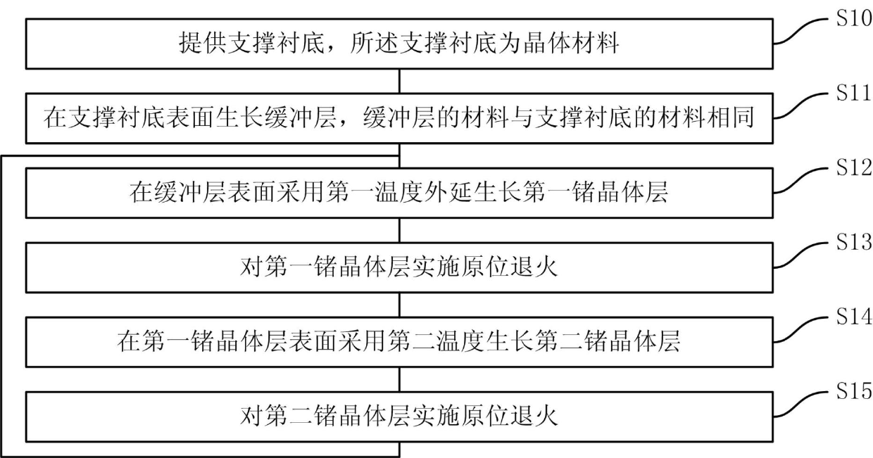
[0021] attached figure 1 Shown is a schematic diagram of the implementation steps of the first embodiment of the present invention, including: step S10, providing a support substrate, the support substrate is a crystal material; step S11, growing a buffer layer on the surface of the support substrate, the material of the buffer layer The same material as the supporting substrate; step S12, epitaxially growing the first germanium crystal layer on the surface of the buffer layer at the first temperature; step S13, implementing in-situ annealing on the first germanium crystal layer; step S14, growing the first germanium crystal layer on the first germanium crystal layer A second germanium crystal layer is grown on the surface at a second temperature, and the first temperature is lower than the second temperature; step S15 , performing in-situ annealing on the second germanium crystal layer.

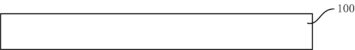
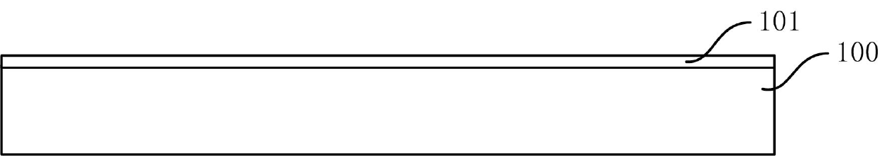
[0022] attached Figure 2A to attach Figure 2D Shown is the process schematic diagram...

no. 2 Embodiment approach

[0032] attached image 3 Shown is a schematic diagram of the implementation steps of the second embodiment of the present invention, including: step S30, providing a support substrate, the support substrate is a crystal material; step S31, growing a buffer layer on the surface of the support substrate, the material of the buffer layer The same material as the supporting substrate; step S32, epitaxially growing the first germanium crystal layer on the surface of the buffer layer at the first temperature; step S33, implementing in-situ annealing on the first germanium crystal layer; step S34, growing the first germanium crystal layer on the first germanium crystal layer A second germanium crystal layer is grown on the surface at a second temperature, and the first temperature is lower than the second temperature; step S35, performing in-situ annealing on the second germanium crystal layer; step S36, using the second germanium crystal layer on the surface of the second germanium c...


PUM

PropertyMeasurementUnit
Thicknessaaaaaaaaaa
Thicknessaaaaaaaaaa

Abstract

The invention provides a growth method of a germanium substrate. The growth method comprises the following steps of: providing a supporting substrate, wherein the supporting substrate is a crystal material; epitaxially growing a first germanium crystal layer on the surface of the supporting substrate at a first temperature; and epitaxially growing a second germanium crystal layer on the surface of the first germanium crystal layer at a second temperature, wherein the first temperature is lower than the second temperature. The growth method has the advantages that: a growth process combining low and high-temperature germanium epitaxial growth is provided; firstly, a germanium layer is grown at a low temperature, thus the germanium layer has low epitaxial growth speed, has two-dimensional growth characteristics and is completely relaxed, and the thin low-temperature germanium layer has multiple defects and is easy for stress relaxing and dislocation annihilation; and then, a germanium epitaxial layer is grown at a high temperature, thus the germanium layer has high growth speed, and a single crystal germanium layer which has high crystal quality and is completely relaxed can be obtained.

Description

technical field [0001] The invention relates to a growth method of a germanium substrate and a germanium substrate, in particular to a growth method of a germanium substrate with high crystal quality and a germanium substrate. Background technique [0002] The chip manufacturing industry is still following Moore's Law and is developing in the direction of 450 mm large-size wafers, nanoscale lithography line width, high precision, high efficiency, and low cost. Since 2004, many top international semiconductor manufacturers have adopted the 90 nm process to produce integrated circuit IC chips. The launch of the 90 nm process marks that the chip manufacturing industry has entered the era of nanotechnology in the range of 100 nm to 0.1 nm. However, severe challenges have been encountered in further improving the integration level and operating speed of chips and reducing the feature size of integrated circuits. The existing materials and processes are approaching their physical ...

Claims


Application Information

Patent Timeline
IPC IPC(8): C30B25/02C30B29/08
Inventor 魏星薛忠营曹共柏张峰张苗王曦
Owner SHANGHAI SIMGUI TECH
Why Eureka
Try Eureka