Preparation method of nano-imprinting composite template

A composite template and nano-imprint technology, applied in the field of micro-nano processing, can solve the problems of slow electron beam direct writing speed and high cost

Inactive Publication Date: 2012-03-28
NANJING UNIV
View PDF4 Cites 14 Cited by
  • Summary
  • Abstract
  • Description
  • Claims
  • Application Information

AI Technical Summary

Problems solved by technology

Templates are usually prepared using electron beam direct writing

Method used


Image

  • Preparation method of nano-imprinting composite template
  • Preparation method of nano-imprinting composite template
  • Preparation method of nano-imprinting composite template

Examples


Embodiment Construction

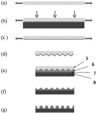
[0019] The present invention will be described in further detail below in conjunction with the accompanying drawings and embodiments.

[0020] The preparation of composite template of the present invention mainly comprises and is divided into following steps:

[0021] (1) Preparation and support of polydimethylsiloxane flakes.

[0022] a) After uniformly mixing component A and component B of SYLGARD? 184 polydimethylsiloxane precursor of Dow Corning Corporation in the United States at a mass ratio of 10:1, spin-coat it on the anti-sticking treated silicon wafer at a speed of 300RPM ;

[0023] b) Put a spin-coated polydimethylsiloxane silicon wafer in a vacuum drying oven, evacuate to 0.5 atm, keep the temperature at 65 degrees, and cure after 5 hours of heat preservation;

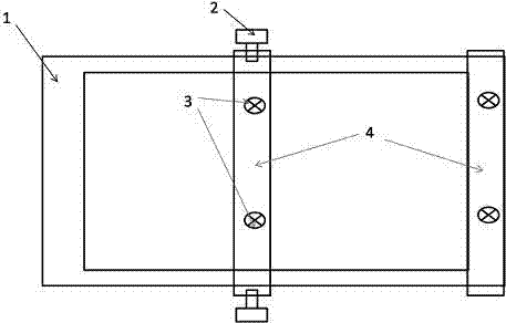
[0024] c) Divide the cured polydimethylsiloxane sheet into strips using a ruler and a blade;

[0025] d) use as figure 1 The clamp shown holds the polydimethylsiloxane sheet and stretches the sheet as r...


PUM


Abstract

The invention belongs to the field of a nano-imprinting technology, and particularly discloses a preparation method of a nano-imprinting composite template. The method comprises the following steps of: stretching a polydimethylsiloxane sheet with stretching equipment; spinning an ultraviolet curing glue on a monocrystalline silicon wafer, and covering the stretched polydimethylsiloxane sheet on the surface of the silicon wafer spinned with the glue, and sufficiently absorbing the ultraviolet curing glue; forming a hard layer on the polydimethylsiloxane surface by the curing of the ultravioletcuring glue, and shrinking the stretched polydimethylsiloxane to form a pattern; and finally, etching with a reaction particle beam, forming bonding on the composite pattern, and performing anti-sticking treatment on the surface to obtain a nano-imprinting composite template with a low cost and an adjustable micro-nano size.

Description

technical field [0001] The invention belongs to the field of micro-nano processing, and in particular relates to a method for preparing a composite template in nano-imprinting. Background technique [0002] In the manufacture of large-scale integrated circuits, photolithography is the most widely used process, including yellow light lithography, extreme ultraviolet lithography, electron beam direct writing, immersion lithography, etc. Under the guidance of Moore's Law, large-scale integrated circuits have steadily entered the nanometer era, and lithography has formed a bottleneck at the 45 nm node. Due to the inherent limitations of optical lithography technology, it has been difficult to meet the rapid development of the semiconductor industry along Moore's Law. Among the next-generation image transfer technologies, electron beam direct writing, X-ray exposure and nanoimprinting technologies play an important role. Among them, the nanoimprint technology was first proposed...

Claims


Application Information

Patent Timeline
IPC IPC(8): G03F7/00
Inventor 宣艳唐晗刘世镇袁长胜葛海雄陈延峰
Owner NANJING UNIV
Why Eureka
Try Eureka